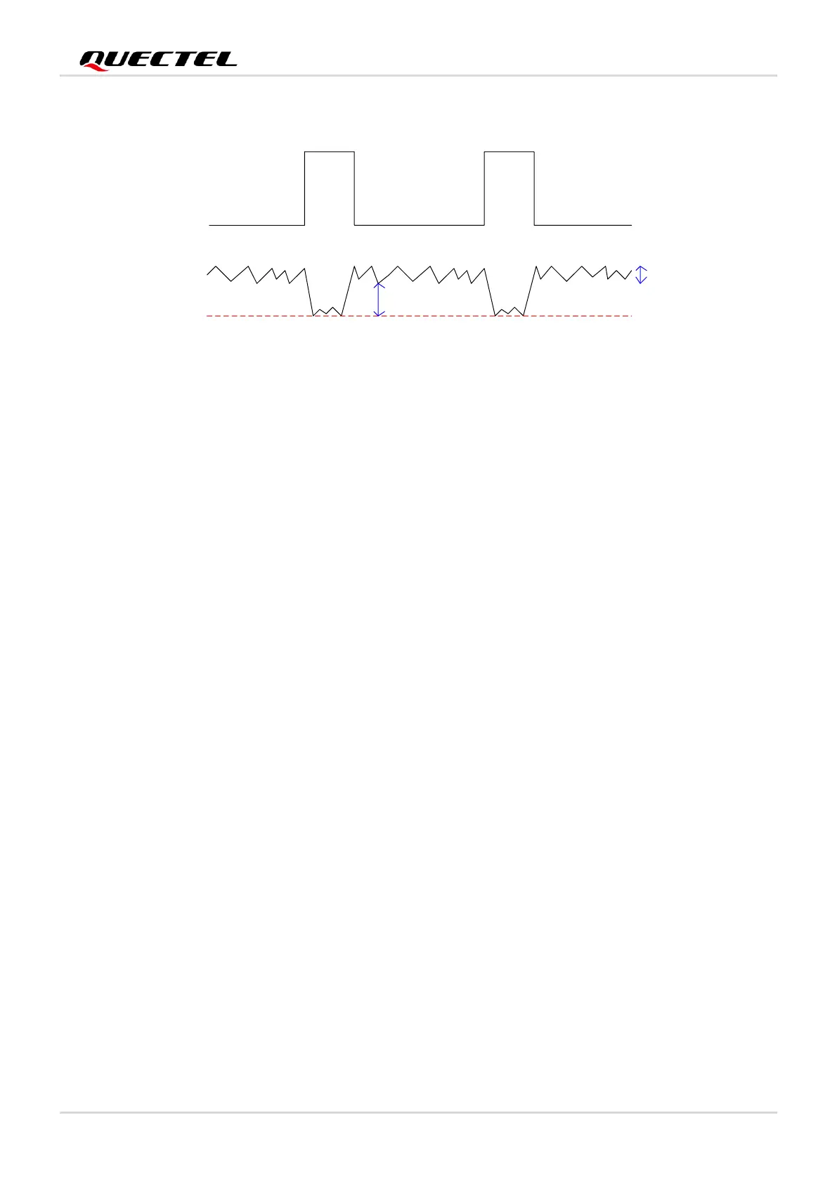
Figure 9: Power Supply Limits during Burst Transmission
To decrease the voltage drop, use a decoupling capacitor of about 100 μF with low ESR and reserve a
decoupling capacitor of about 100 μF. In addition, a multi-layer ceramic chip (MLCC) capacitor array
should also be reserved due to its ultra-low ESR. It is recommended to use 16 ceramic capacitors for
composing the MLCC array, and place these capacitors close to VBAT pins. The main power supply from
an external application must be a single voltage source and can be expanded to two sub paths with the
star structure. The width of VBAT_BB trace should be not less than 2 mm and the width of VBAT_RF1 and
VBAT_RF2 trace should be not less than 2 mm. In principle, the longer the VBAT trace is, the wider it
should be.
In addition, in order to ensure the stability of the power supply, it is necessary to add a high-power TVS at
the front end of the power supply. Reference circuit is shown as below: