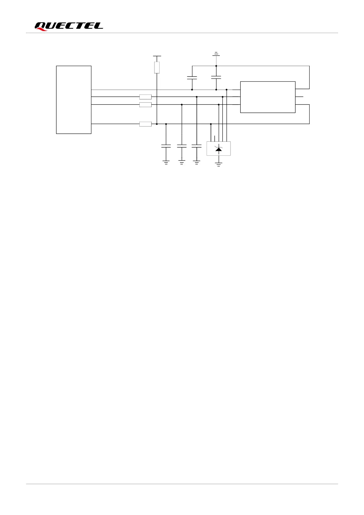
Figure 21: Reference Circuit of (U)SIM Interface with a 6-pin (U)SIM Card Connector
To enhance the reliability and availability of the (U)SIM card in applications, follow the criteria below in
(U)SIM circuit design.
⚫ Keep (U)SIM card connector as close as possible to the module. Keep the trace length as short as
possible, at most 200 mm.
⚫ Keep (U)SIM card signal traces away from RF and VBAT traces.
⚫ To avoid cross-talk between USIM_DATA and USIM_CLK, keep them away from each other and
shield them with ground surrounded.
⚫ To offer better ESD protection, add a TVS array with parasitic capacitance not exceeding 10 pF. Add
0 Ω resistors in series between the module and the (U)SIM card connector so as to suppress EMI
spurious transmission and enhance ESD protection. The 10 pF capacitors are used to filter out RF
interference.
⚫ The 20 kΩ pull-up resistor on USIM_DATA trace improves anti-jamming capability and should be
placed close to the (U)SIM card connector.
⚫ A space has been reserved for eSIM inside the module on the (U)SIM2 interface.
⚫ All these resistors, capacitors and TVS should be close to (U)SIM card connector in PCB layout.
4.4. I2C Interface
The module provides one I2C interface. As an open drain output, it should be pulled up to 1.8 V.
Pin definition is listed as follows:


 To Next Page