EasyManua.ls Logo

Quectel RG520N-AT - Pcie Interface

Quectel RG520N-AT
114 pages
Print Icon
To Next Page IconTo Next Page
To Previous Page IconTo Previous Page
Loading...
5G Module Series
RG520N-AT_Hardware_Design 62 / 109
VCCA VCCB
OE
A1
A2
A3
A4
NC
GND
B1
B2
B3
B4
NC
VDD_EXT
SPI_CS
SPI_CLK
SPI_MISO
SPI_MOSI
0.1 μF
0.1 μF
SPI_CS_N_MCU
SPI_CLK_MCU
SPI_MISO_MCU
SPI_MOSI_MCU
VDD_MCU
Translator
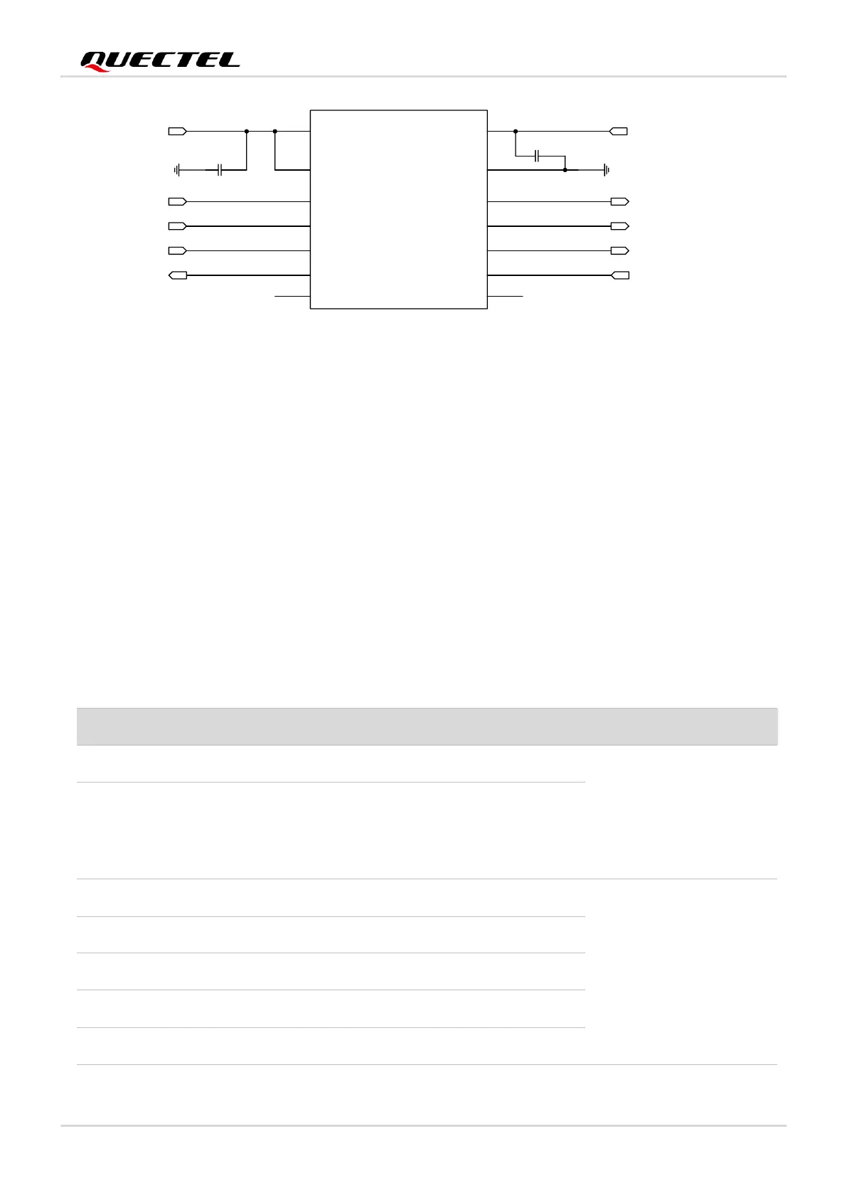
Figure 31: Reference Circuit of SPI with a Voltage-level Translator
4.11. PCIe Interface
The module provides one integrated PCIe (Peripheral Component Interconnect Express) interface. The
key features of the PCIe interface are mentioned below:
PCI Express Specification Revision 3.0 compliance.
Data rate at 8 Gbps per lane for PCIe 3.0.
Used to connect to an external Ethernet IC (MAC and PHY) or Wi-Fi IC.
Table 26: Pin Definition of PCIe Interface
Pin Name
Pin No.
I/O
Description
Comment
PCIE_REFCLK_P
40
AIO
PCIe reference clock (+)
In root complex mode, it is
an output signal.
In endpoint mode, it is an
input signal. Requires
differential impedance of
85 Ω.
PCIE_REFCLK_M
38
AIO
PCIe reference clock (-)
PCIE_TX0_M
44
AO
PCIe transmit 0 (-)
Requires differential
impedance of 85 Ω.
If unused, keep them
open.
PCIE_TX0_P
46
AO
PCIe transmit 0 (+)
PCIE_TX1_M
41
AO
PCIe transmit 1 (-)
PCIE_TX1_P
43
AO
PCIe transmit 1 (+)
PCIE_RX0_M
32
AI
PCIe receive 0 (-)

Table of Contents

Related product manuals