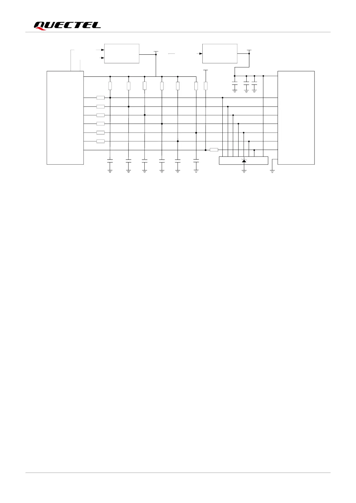
Figure 30: Reference Circuit of SDIO Interface
In SDIO interface design, in order to ensure good communication performance with SD card, the following
design principles should be complied with:
⚫ The voltage range of SD power supply VDD_2V95 is 2.7–3.6 V and a sufficient current of up to 0.8 A
should be provided. SDIO_VDD_DUAL is an SDIO bus power domain, which can be used for SD
card I/O signals pull-up. Note that SDIO_VDD is an input pin of the module.
⚫ To avoid jitter of bus, pull up SDIO_CMD and SDIO_DATA[0:3] to SDIO_VDD_DUAL with resistors
R7 to R11. The resistance can be 10–100 kΩ and 100 kΩ is recommended.
⚫ To improve signal quality, add 0 Ω resistors R1 to R6 in series between the module and the SD card
connector. The bypass capacitors C1 to C6 are reserved and not mounted by default. All resistors
and bypass capacitors should be placed close to the SD card connector.
⚫ For good ESD protection, add ESD protection components with capacitance value less than 1.2 pF
on each SD card pin.
⚫ Route the SDIO signal traces at inner layer with ground surrounded. The impedance of SDIO data
trace is 50 Ω (±10 %).
⚫ Keep SDIO signals far away from other sensitive circuits/signals such as RF circuits, analog signals,
as well as noise signals such as clock signals and DC-DC signals.
⚫ Keep the trace length difference between SDIO_CLK and SDIO_DATA[0:3]/SDIO_CMD less than
2 mm and the total routing length less than 50 mm for SDR104 mode. For other speed modes, the
trace length difference between SDIO_CLK and SDIO_DATA[0:3]/SDIO_CMD should be less than
6 mm and the total trace routing length less than 150 mm.
⚫ Make sure the adjacent trace spacing is twice the trace width and the load capacitance of SDIO bus
should be less than 5.0 pF.
⚫ The DETECTIVE pin of SD card connector must be connected to the module when the SD card
function is being used.
 Loading...


