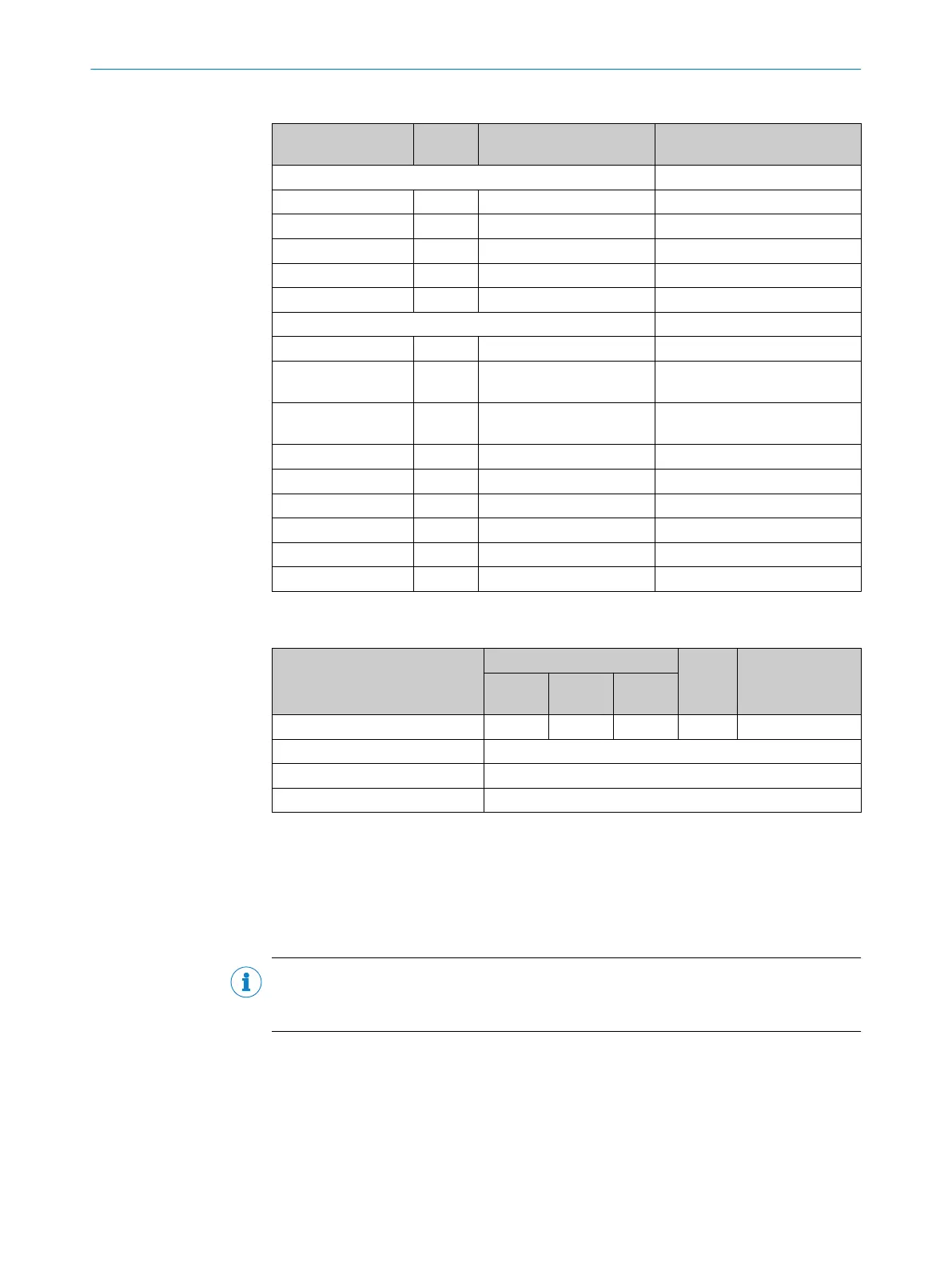
Table 187: Serial interface block signals
Pin name Model
name
Function Note
Host interface
clk Input Clock input
spi_miso output SPI data output
spi_mosi Input SPI data input
spi_clk Input SPI clock
spi_sel Input SPI selection
IP Core interface
rst Input Internal reset Connect to IUO(1) of the IP Core
bit_period(2:0) Input Internal state machine Connect to IUO(4:2) of the IP
Core
online_sta‐
tus_d(15:0)
Input Internal status IP Core
hostd_a(6:0) output Register block address bus
hostd_di(7:0) output Data bus interface to core
hostd_do(7:0) Input Data bus core to interface
hostd_r output Read access requirement
hostd_w output Write access requirement
hostd_f output Freeze register selection
The signal characteristics of the serial interface block are set out in the table below:
Table 188: SPI interface characteristics
Parameter Value Units Comments
Mini‐
mum
Typical Maxi‐
mum
Clock spi_clk 10 MHz
Clock phase (PHA) PHA = 1, scanning during falling clock edge
Clock polarity (POL) POL = 0, base value of the clock is 0
Data endianness MSB is clocked out first
The SPI interface block implements the following register based transactions:
•
Read individual register
•
Read several registers with random access
•
Write to individual register
•
Write to several registers (automatic increment)
•
Read/write sequence
NOTE
It must be noted that during a read/write sequence, the write operation must always be
the final transaction.
At the beginning of each transaction, the DSL Master transmits the online-status via
spi_miso in two bytes.
9.2.1 Time control of the SPI
When accessing the SPI interface, the following specifications for time control must be
adhered to:
FPGA IP-CORE 9
8017595/ZTW6/2018-01-15 | SICK T E C H N I C A L I N F O R M A T I O N | HIPERFACE DSL
®
141
Subject to change without notice
 Loading...