7SR18 Description Of Operation
Unrestricted ©2018 Siemens Protection Devices Limited Page 5 of 78
List of Figures
Figure 1.4-1 Functional Diagram of 7SR18 Non-Directional Three-Phase and Earth .......................................... 10
Figure 1.4-2 Connections Diagram for 7SR18 Non-Directional Relay (3BI and 5BO) .......................................... 11
Figure 1.4-3 Connections Diagram for 7SR18 Non-Directional Relay (6BI and 8BO) .......................................... 12
Figure 1.4-4 Functional Diagram of 7SR18 Directional Three-Phase and Earth .................................................. 13
Figure 1.4-5 Connections Diagram for 7SR18 Directional Relay (3BI and 5BO) ................................................. 14
Figure 1.4-6 Connections Diagram for 7SR18 Directional Relay (6BI and 8BO) ................................................. 15
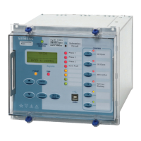
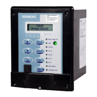
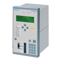
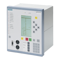
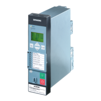
Figure 2.2-1 Front View of Relay ...................................................................................................................... 17
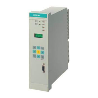
Figure 2.2-2 Rear view of Relay ....................................................................................................................... 17
Figure 2.2-3 Earth connection Symbol .............................................................................................................. 17
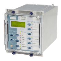
Figure 2.3-1 Relay with transparent cover ......................................................................................................... 18
Figure 2.5-1 Relay with Transparent cover removed ......................................................................................... 19
Figure 2.5-2 Close up of Typical Relay Label .................................................................................................... 20
Figure 2.5-3 Typical Relay Identifier LCD Text .................................................................................................. 21
Figure 2.5-4 LED Indication Label .................................................................................................................... 22
Figure 2.8-1 Binary Input Logic ......................................................................................................................... 24
Figure 2.9-1 Binary Output Logic ...................................................................................................................... 25
Figure 2.11-1 Start-up Counter Meter ............................................................................................................... 26
Figure 2.11-2 Unexpected Restarts Lockout Text .............................................................................................. 26
Figure 2.11-3 Typical Start-up Events Text ....................................................................................................... 27
Figure 3.1.1-1 Biased Differential Characteristic (Offset Disabled) ..................................................................... 28
Figure 3.1.1-2 Biased Differential Characteristic (Offset Enabled - Default) ........................................................ 29
Figure 3.1.1-3 Logic Diagram: Biased Current Differential Protection ................................................................. 29
Figure 3.1.2-1 Differential Highset Characteristic............................................................................................... 30
Figure 3.1.2-2 Logic Diagram: Differential High Set Current Protection .............................................................. 30
Figure 3.1.3-1 Logic Diagram: Protection Communications Signalling Supervision ............................................. 31
Figure 3.3.1-1 Logic Diagram: Directional Overcurrent Element (67) .................................................................. 33
Figure 3.3.2-1 Logic Diagram: Instantaneous Over-current Element .................................................................. 34
Figure 3.3.3-1 Logic Diagram: Time Delayed Overcurrent Element .................................................................... 36
Figure 3.3.4-1 Logic Diagram: Voltage Controlled Overcurrent Element ............................................................. 37
Figure 3.4.1-1 Logic Diagram: Derived Directional Earth Fault Protection........................................................... 38
Figure 3.4.2-1 Logic Diagram: Derived Instantaneous Earth Fault Element ........................................................ 39
Figure 3.4.3-1 Logic Diagram: Derived Time Delayed Earth Fault Element ........................................................ 40
Figure 3.5.1-1 Logic Diagram: Measured Earth Fault Protection ........................................................................ 41
Figure 3.5.2-1 Logic Diagram: Measured Instantaneous Earth-fault Element ...................................................... 42
Figure 3.5.3-1 Logic Diagram: Measured Time Delayed Earth Fault Element (51G) ........................................... 43
Figure 3.6-1 Logic Diagram: Cold Load Settings (51c)....................................................................................... 44
Figure 3.7-1 Logic Diagram: Negative Phase Sequence Overcurrent (46NPS) ................................................... 45
Figure 3.8-1 Logic Diagram: Phase Current Inputs Undercurrent Detector (37) .................................................. 46
Figure 3.8-2 Logic Diagram: Earth Current Inputs Undercurrent Detector (37G) ................................................. 46
Figure 3.9-1 Logic Diagram: Thermal Overload Protection (49).......................................................................... 48
Figure 3.10-1 Logic Diagram: 50G Line Check Elements (50G LC) .................................................................... 48
Figure 3.10-2 Logic Diagram: 50 Line Check Elements (50LC) .......................................................................... 48
Figure 4.1.2-1 Typical Sequence with 3 Instantaneous and 1 Delayed trip ......................................................... 51
Figure 4.6-1 Basic Auto-Reclose Sequence Diagram ........................................................................................ 56
Figure 4.8-1 Logic Diagram: Circuit Breaker Status ........................................................................................... 59
Figure 4.9-1 Sequence Diagram: Quick Logic PU/DO Timers (Counter Reset Mode Off) .................................... 61
Figure 5.1-1 Logic Diagram: Circuit Breaker Fail Protection (50BF) ................................................................... 62
Figure 5.2-1 Logic Diagram: Circuit Breaker Fail Protection (50BF) ................................................................... 64
Figure 5.3.1-1 Logic Diagram: CT Supervision Function (60CTS-I) .................................................................... 65
Figure 5.3.2-1 Logic Diagram: CT Supervision Function (60CTS) ...................................................................... 66
 Loading...