International English 3 Commissioning
MICROMASTER 440 Operating instructions
6SE6400-5CA00-0BP0
33
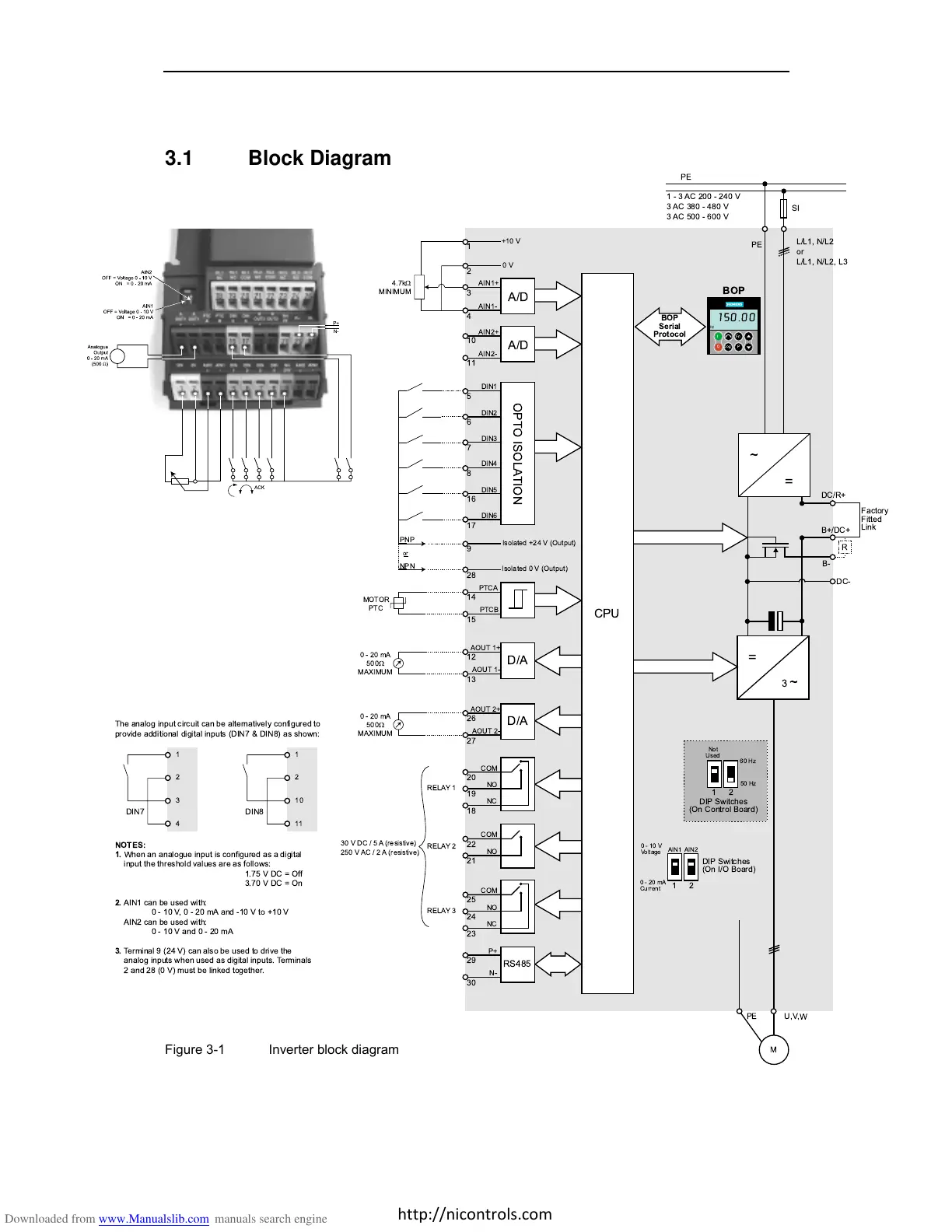
PE
1 - 3 AC 200 - 240 V
3 AC 380 - 480 V
3 AC 500 - 600 V
SI
PE
L/L1, N/L2
or
L/L1, N/L2, L3
~
=
=
3
~
B+/DC+
DC/R+
Factory
Fitted
Link
B-
R
DC-
PE U,V,W
M
12
DIP Switches
(On I/O Board)
AIN1 AIN2
0 - 10 V
Voltage
0 - 20 mA
Current
12
DIP Switches
(On Control Board)
60 Hz
50 Hz
Not
Used
Jog
0
I
P
Fn
Hz
150.00
A/D
A/D
1
2
3
4
10
11
5
6
7
8
16
17
+10 V
0V
AIN1+
AIN1-
AIN2+
AIN2-
DIN1
DIN2
DIN3
DIN4
DIN5
DIN6
PTCA
PTCB
MOTOR
PTC
0-20mA
500
W
MAXIMUM
0-20mA
500
W
MAXIMUM
RELAY 1
RELAY 2
AOUT 1+
AOUT 1-
AOUT 2+
AOUT 2-
4.7k
W
MINIMUM
9
28
14
15
12
13
26
27
Isolated +24 V (Output)
Isolated 0 V (Output)
NPN
PNP
or
OPTO ISOLATION
CPU
P+
N-
29
30
COM
NC
20
18
NO
19
RELAY 3
RS485
COM
NC
25
23
NO
24
COM
22
NO
21
D/A
D/A
The analog input circuit can be alternatively configured to
provide additional digital inputs (DIN7 & DIN8) as shown:
NOTES:
1.
When an analogue input is configured as a digital
input the threshold values are as follows:
2.
AIN1 can be used with:
0-10V,0-20mAand-10Vto+10V
AIN2 can be used with:
0-10Vand0-20mA
3.
Terminal 9 (24 V) can also be used to drive the
analog inputs when used as digital inputs. Terminals
2 and 28 (0 V) must be linked together.
1
2
10
11
DIN8
1
2
3
4
DIN7
BOP
1.75VDC=Off
3.70VDC=On
30 V DC / 5 A (resistive)
250 V AC / 2 A (resistive)
Ω
BOP
Serial
Protocol
3.1 Block Diagram
Figure 3-1 Inverter block diagram
http://nicontrols.com
 Loading...