NOTICE
Damage to the module
If the outputs are overloaded, the heat can melt the contacts.
Therefore, for a demand factor of 100%, a max. current of I
out
= 0.25 A at X111, X222, X333:
Pin 2, must not be exceeded.
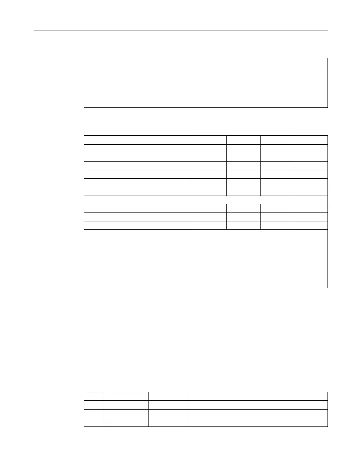
Table 12-27 Electrical specication of the digital outputs
Digital outputs min. Standard max. Nominal
High-level voltage (U
H
) V
CC
- 3 V
1)
V
CC
24 V
Output current I
OUT
- - 250 mA
2)
-
Voltage with low level (U
L
) - - - Output open
Leakage current at low level - 50μA 400μA -
Signal delay time T
PHL
- 0.5 ms - -
Internal resistance R
I
-- 7 kΩ/kOhm -- --
Maximum switching frequency
Resistive load - - 100 Hz -
Inductive load - - 2 Hz -
Lamp - - 11 Hz -
1) U
H_typical
= V
CC
- I
OUT
× R
ON
V
CC
: Current operating voltage
I
OUT
: Output current
Maximum short-circuit current: 4 A (max. 100 μs, V
CC
= 24 V)
R
ON
: Maximum internal resistance = 0.4 Ω
2) For a simultaneity factor of 100% (all outputs active)
Incorrect connection causes neither high level nor destruction of the outputs.
12.2.3.5 X3 analog inputs/outputs
Analog X3 inputs/outputs
X3 pin assignment
The analog signal to be measured is connected to the terminals AI 1+/- and AI 2+/-. The CO and
CI terminals supply the constant current for the 4-wire measurement of PT100 elements:
Table 12-28 Pin assignment (standard)
Pin Signal name Signal type Meaning
1 CO1 O Channel 1 current output for PT100
2 CI1 I Channel 1 current input for PT100
3 AI1+ I Channel 1 analog input +
Connectable components
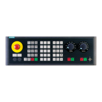
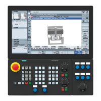
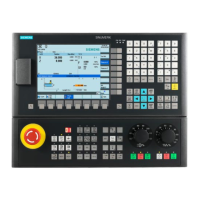
12.2PP 72/48D PN and PP 72/48D 2/2A PN
NCU 1750
Equipment Manual, 10/2023, A5E45627807B AH 131
 Loading...