SN8P2624
8-Bit Micro-Controller
SONiX TECHNOLOGY CO., LTD Page 77 Version 0.3
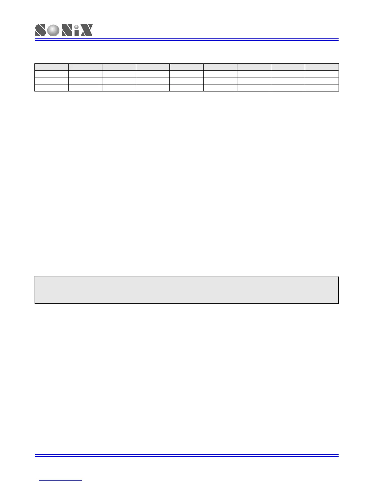
8.3.2 TC1M MODE REGISTER
0DCH Bit 7 Bit 6 Bit 5 Bit 4 Bit 3 Bit 2 Bit 1 Bit 0
TC1M
TC1ENB TC1rate2 TC1rate1 TC1rate0 TC1CKS ALOAD1 TC1OUT PWM1OUT
Read/Write R/W R/W R/W R/W R/W R/W R/W R/W
After reset 0 0 0 0 0 0 0 0
Bit 0 PWM1OUT: PWM output control bit.
0 = Disable PWM output.
1 = Enable PWM output. PWM duty controlled by TC1OUT, ALOAD1 bits.
Bit 1 TC1OUT: TC1 time out toggle signal output control bit. Only valid when PWM1OUT = 0.
0 = Disable, P5.3 is I/O function.
1 = Enable, P5.3 is output TC1OUT signal.
Bit 2 ALOAD1: Auto-reload control bit. Only valid when PWM1OUT = 0.
0 = Disable TC1 auto-reload function.
1 = Enable TC1 auto-reload function.
Bit 3 TC1CKS: TC1 clock source select bit.
0 = Internal clock (Fcpu or Fosc).
1 = External clock from P0.1/INT1 pin.
Bit [6:4] TC1RATE[2:0]: TC1 internal clock select bits.
000 = fcpu/256.
001 = fcpu/128.
…
110 = fcpu/4.
111 = fcpu/2.
Bit 7 TC1ENB: TC1 counter control bit.
0 = Disable TC1 timer.
1 = Enable TC1 timer.
Note: When TC1CKS=1, TC1 became an external event counter and TC1RATE is useless. No more P0.1
interrupt request will be raised. (P0.1IRQ will be always 0).