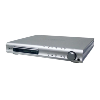
HCD-SLK10D/SLK20D
66
MAIN BOARD IC100 R5F364AMDFA (SYSTEM CONTROLLER)
Pin No. Pin Name I/O Description
1 HP MUTE O Headphone muting on/off control signal output terminal “L”: muting on
2 HP DET I Headphone detection signal input terminal “H”: headphone is connected
3 BUZZER CONT O Buzzer level control signal output terminal
4 SIRCS IN I SIRCS signal input from remote control receiver
5 DVD_SOD O Serial data output to the servo DSP
6 DVD_SID I Serial data input from the servo DSP
7 DVD SCO I Serial data transfer clock signal input from the servo DSP
8 BYTE I External data bus width selection signal input terminal
9 CNVSS I Processor mode selection signal input terminal
10 XCIN I Sub system clock (32.768 kHz) input terminal
11 XCout O Sub system clock (32.768 kHz) output terminal
12 RESET I
System reset signal input from the reset signal generator “L”: reset
For several hundreds msec. after the power supply rises, “L” is input, then it change to “H”
13 XOUT O Main system clock (5 MHz) output terminal
14 VSS - Ground terminal
15 XIN I Main system clock (5 MHz) input terminal
16 VCC - Power supply terminal (+3.3V)
17 NO USE I Not used
18 RDS-INT I RDS interrupt signal input from the tuner (FM/AM)
19 PROTECT-INT I Protect interrupt signal input from switching regulator
20 /AC-CUT I AC cut detection signal input terminal
21 XSYSRST O Reset signal output to the servo DSP “L”: reset
22 NO_USE - Not used
23 KEY_LED_ON - Not used
24 TRG-SW I Trigger detection switch input terminal
25 DVD_XIFBUSY O Busy signal output to the servo DSP
26 TP BUZZER O Buzzer signal output terminal
27 XIFCS O Chip select signal output to the servo DSP
28 SONYLOGO LED O LED drive signal output terminal for SONY logo indicator “H”: LED on
29 IIC-CLK I/O Two-way I2C clock bus terminal Not used
30 IIC-DATA I/O Two-way I2C data bus terminal Not used
31 TXD OUT O Serial data output terminal Not used
32 RXD IN I Serial data input terminal Not used
33 CLK1 O Serial data transfer clock signal output terminal Not used
34 RTS1 I Return to send signal input terminal Not used
35 AML TXD OUT O Serial data output to the audio DSP
36 AML RXD IN I Serial data input from the audio DSP
37 AML RESET O Reset signal output to the audio DSP “L”: reset
38 AML BUSY I Busy signal input from the audio DSP
39 (CLKOUT) O Clock signal output terminal Not used
40 TROPENPWM O Not used
41 (PULL DOWN) I Fixed at “L” in this set
42 CKSW1 I Chucking detection switch input terminal
43 OCSW1 I Disc in/out detection switch input terminal
44 REV O Loading motor drive signal output terminal (reverse direction)
45 FWD O Loading motor drive signal output terminal (forward direction)
46 (PULL_UP) - Fixed at “H” in this set
47 TP SDA I/O Two-way data bus with the TOUCH SENSOR board
48 TP SCL O Serial data transfer clock signal output to the TOUCH SENSOR board
49 EEPROM-DATA I/O Two-way data bus with the EEPROM
50 EEPROM-CLK O Serial data transfer clock signal output to the EEPROM
51 /D-AMP-RESET O Reset signal output to the digital power amplifi er “L”: reset
52, 53 /OTW1, /OTW2 I Over temperature warning signal input from the digital power amplifi er
54 PROTECT AMP I Protect signal input terminal
55 READY I Ready signal input from the digital power amplifi er
56 /CLIP I Clipping warning signal input from the digital power amplifi er
57 USB OC I VBUS over current detection signal input terminal for USB connector
58 NO USE - Not used
 Loading...