80
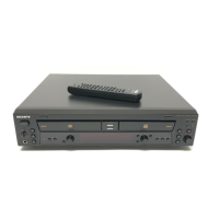
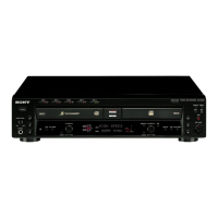
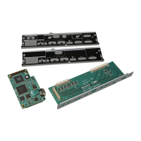
RCD-W10
Pin No.
139
140
141
142
143
144
145
146
147
148
149
150
151
152
153
154
155
156
157
158
159
160
161, 162
163
164
165
166
167
168
169
170
171
172
173
174
175
176
177
178
179
180
181
182
183
184
185
186
187
188
189
I/O
—
O
I/O
I/O
I
O
O
I
O
I
—
—
I
I
O
—
—
—
—
O
I
I
I
O
O
O
I
I
O
O
I
I
—
—
I/O
O
—
—
O
O
O
O
—
—
I
O
O
I
I
I
Pin Name
DVSS
ATIPSYNC
BIDATA
BICLK
WOBBLE
JITERR
JITPCO
JITLPFI
JITLPFO
JITVCOIN
AVSS
AVDD
DIRRS
DIRVCO
DIRLPF
AVDD
AVSS
DVDD
DVSS
DIRERR
DIN1
DIN2
DIN3, DIN4
DACCKOUT
ENCCKOUT
CDCKOUT
AUXMCKIN
XTALCK
XTAL
PDO0
VCNT0
R0
AVDD
AVSS
TEST4
ROUT
AVDD
AVSS
LOUT
DACDATA
DACLRCK
DACBCK
DVDD
DVSS
ADCDATA
ADCBCK
ADCLRCK
AUXDATA
AUXBCK
AUXLRCK
Description
Ground terminal (digital)
ATIP sync signal output
ATIP demodulator input/output (fixed at “L”)
ATIP demodulator input/output (fixed at “L”)
ATIP demodulator input/output
Clock jitter suppressor error signal output Not used (open)
PLL phase frequency comparator output
PLL low-pass filter input terminal
PLL low-pass filter output terminal
PLL, VCO clock input terminal
Ground terminal (analog)
Power supply +3.3V (analog) for the clock jitter suppressor
VCO gain control signal input
VCO free running oscillation frequency control signal input
Loop filter setting terminal
Power supply +3.3V (analog) for the DIR
Ground terminal (analog)
Power supply +5V (digital)
Ground terminal (digital)
PLL lock data error output
Digital data input from the IC500
Digital data input from the IC101
Digital data input Not used (open)
DAC clock output Not used (open)
RF processor clock output Not used (open)
CD decoder clock output Not used (open)
External clock input (fixed at “L”)
Crystal oscillation circuit input
Crystal oscillation circuit output
Charge pump output
VCO control voltage input
VCO bias resistor terminal
Power supply +3.3V (analog) for the clock
Ground terminal (analog)
ADCCKOUT clock output
DAC output Not used (open)
Power supply +5V (analog) for the internal DAC
Ground terminal (analog)
DAC output Not used (open)
DAC serial data output Not used (open)
DAC LRCK output Not used (open)
DAC BCK output Not used (open)
Power supply +3.3V (digital)
Ground terminal (digital)
ADC serial data input Not used (fixed at “L”)
ADC BCK output Not used (open)
ADC LRCK output Not used (open)
External serial data input Not used (open)
External BCK input Not used (fixed at “L”)
External LRCK input Not used (fixed at “L”)
 Loading...