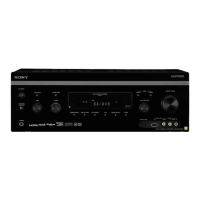
STR-DA6400ES
161
Pin No. Pin Name I/O Description
N3 MM_WE_N O Write enable signal output to the SD-RAM
N4 MM_ADDR08 O Address signal output to the SD-RAM
N5 VDD - Power supply terminal (+1.3V)
N11 to N16 VSS - Ground terminal
N22 VCCP - Power supply terminal (+3.3V)
N23 to
N26
PCI_AD17, PCI_
TRDY_N, PCI_IRDY_N,
PCI_FRAME_N
I/O Two-way data bus with terminal Not used
P1 MM_ADDR07 O Address signal output to the SD-RAM
P2 VSS - Ground terminal
P3 MM_ADDR01 O Address signal output to the SD-RAM
P4 MM_BA1 O Bank select signal output to the SD-RAM
P5 VDD - Power supply terminal (+1.3V)
P11 to P16 VSS - Ground terminal
P22 VCCP - Power supply terminal (+3.3V)
P23 PCI_PERR_N I/O Two-way data bus with terminal Not used
P24 PCI_STOP_N I/O Two-way data bus with terminal Not used
P25 VSS - Ground terminal
P26 PCI_DEVSEL I/O Two-way data bus with terminal Not used
R1, R2
MM_ADDR06,
MM_ADDR00
O Address signal output to the SD-RAM
R3 VCCM - Power supply terminal (+3.3V)
R4 MM_BA0 O Bank select signal output to the SD-RAM
R5 VCCM - Power supply terminal (+3.3V)
R11 to R16 VSS - Ground terminal
R22 VDD - Power supply terminal (+1.3V)
R23 PCI_C/BE1_N O
Write enable signal output to the parallel/serial converter, parallel bus/I2C bus converter and
fl ash rom
R24 PCI_PAR I/O Two-way data bus with terminal Not used
P25 PCI_SERR_N I/O Two-way data bus with terminal Not used
R26 PCI_AD15 I/O Two-way data bus with terminal Not used
T1 MM_ADDR05 O Address signal output to the SD-RAM
T2 VSS - Ground terminal
T3, T4
MM_ADDR02,
MM_ADDR10
O Address signal output to the SD-RAM
T5 VCCM - Power supply terminal (+3.3V)
T11 to T16 VSS - Ground terminal
T22 VDD - Power supply terminal (+1.3V)
T23 to T26
PCI_AD10, PCI_AD12
to PCI_AD14
I/O Two-way data bus with terminal Not used
U1 VCCM - Power supply terminal (+3.3V)
U2 MM_DQM3 O Data mask signal output to the SD-RAM
U3, U4
MM_ADDR04,
MM_ADDR03
O Address signal output to the SD-RAM
U5 VSS - Ground terminal
U22 VSS - Ground terminal
U23, U24 PCI_AD08, PCI_AD09 I/O Two-way data bus with terminal Not used
U25 VSS - Ground terminal
U26 PCI_AD11 I/O Two-way data bus with terminal Not used
V1 MM_DQS3 I/O Two-way data strobe signal with the SD-RAM
V2 VCCM - Power supply terminal (+3.3V)
V3 MM_DQM2 O Data mask signal output to the SD-RAM
V4 MM_CS1_N O Chip select signal output terminal Not used
V5 VSS - Ground terminal
V22 VSS - Ground terminal
V23 PCI_AD06 I/O Two-way data bus with terminal Not used
V24 VCCP - Power supply terminal (+3.3V)
V25 PCI_C/BE0_N I/O Two-way data bus with terminal Not used
w
w
w
.
x
i
a
o
y
u
1
6
3
.
c
o
m
Q
Q
3
7
6
3
1
5
1
5
0
9
9
2
8
9
4
2
9
8
T
E
L
1
3
9
4
2
2
9
6
5
1
3
9
9
2
8
9
4
2
9
8
0
5
1
5
1
3
6
7
3
Q
Q
TEL 13942296513 QQ 376315150 892498299
TEL 13942296513 QQ 376315150 892498299
http://www.xiaoyu163.com
http://www.xiaoyu163.com