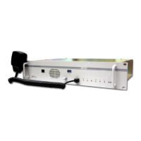
Technical Manual
© SPECTRA ENGINEERING 2006 Revision 4.2.2
130
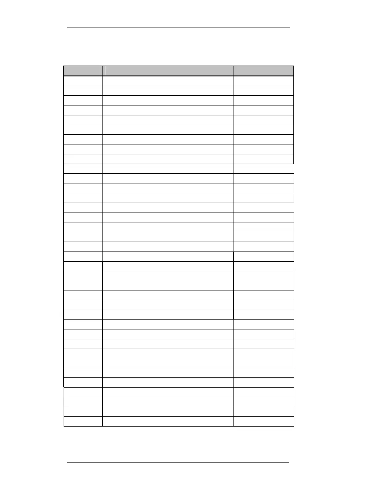
9. Drawings
Drawing No.
Description
Band
Figure 8.1 Receiver Component Overlay All
Figure 8.2 Exciter Component Overlay All
Figure 8.3 Power Amplifier Component Overlay N to Q
Figure 8.4 Micro Controller Component Overlay All
Figure 8.5 VCO Component Overlay A to Q3
Figure 8.6 VCO Component Overlay R to X
Figure 8.7 High Spec Rx VCO Component Overlay A to Q
BD001-1 Receiver Block Diagram All
BD002-1 Exciter Block Diagram All
BD003-1/2 Micro Controller Block Diagram All
BD004-1 Power Amplifier Block Diagram All
IC001-1 MX800 Interconnection Diagram All
CS001-1/6 Micro Controller Board Circuit Diagram All
CS002-1 Exciter Circuit Diagram All
CS003-2 Receiver Front End Circuit Diagram All
CS004-1 TX VCO Circuit Diagram A to Q
CS005-1 RX VCO Circuit Diagram A to Q2
CS010-1 PA 35W Circuit Diagram R to X
CS011-1 TX VCO Circuit Diagram R to X
CS012-1 RX VCO Circuit Diagram R to X
CS015-1/2 Receiver Module Mixer and Programmable 45MHz IF
Section
A & B
CS016-1 Power Amplifier 50W Circuit Diagram A & B
CS017-1/2 Receiver Module Mixer and Programmable IF Section All (except A&B bands)
CS018-1 Isolated Interface Option All
CS021-1 Trunk Interface Circuit diagram All
CS022-1 T11 option PCB Circuit diagram All
CS023-1 HP Rx VCO Circuit Diagram A to Q
CS025-1/2 Receiver Module Mixer and Programmable 70 MHz IF
Section
A3
CS028-1 Wide Band Power Amplifier 50W Circuit Diagram R2
CS029-1 Wide Band Power Amplifier 50W Circuit Diagram N to Q
CS031-1 Wide Band Power Amplifier 50W Circuit Diagram A to B
CS033-1 Wide Band Power Amplifier 50W Circuit Diagram K to M
CS035-1 T29 isolated interface Circuit Diagram ALL
CS037-1 T19/T26 Line encoder/decoder interface All