Do you have a question about the Spectra Engineering MX800 and is the answer not in the manual?
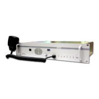
Details the MX800 series as a high-performance radio transceiver.
Provides address, phone, fax, email, and web for Spectra Engineering.
Advises on compliance with FCC rules for digital devices and potential interference.
Lists revisions, versions, chapter changes, and pages changed for the manual.
Outlines general safety precautions for operation, service, and repair.
Lists conditions not covered by the MX800 warranty.
Describes the physical characteristics, modules, and construction of the MX800.
Details the functions of the Exciter, Receiver, Power Amplifier, and Micro Controller modules.
Provides instructions for unpacking and physically installing the MX800 radio.
Outlines the main steps for setting up and operating the MX800 radio.
Describes the option for switchable IF filters for 12.5kHz/25kHz channel spacing.
Describes the provision for fitting a CTCSS encoder/decoder for non-predictive tone decoding.
Details the provision for fitting a full duplex DCS encoder/decoder with 83 digital codes.
Describes the option for transformer-balanced and isolated VF inputs/outputs.
Provides balanced/isolated VF I/O with isolated E (PTT) and M (Mute) leads.
Describes the internally mounted coaxial changeover relay for simplex applications.
Describes an option for RF signal conversion for injection into the receiver for diagnostics.
Provides a 40mS delay to received audio for eliminating mute crash and handling data.
Provides upgraded CTCSS tone suppression on the RX VF by fitting a high-pass filter.
Describes the capability for a Power Save (Low Standby Current) Mode in three stages.
States that this option combines the functions and features of T08, T09, and T10.
Provides for external injection of the TX reference frequency.
Describes the local control option for user interface with speaker, mic, and mute functions.
Describes the local control option for channel selection via front panel switches.
Provides 1PPM frequency stability for narrowband MX800s in K to X bands.
Describes an optional extended operating temperature range version.
Provides flexibility and features for radio base stations with this option board.
Details the installation procedure for the T19/T26 Option PCB and RJ45 Daughter PCB.
Offers selection between 2-wire or 4-wire systems with balanced audio and dual E+M.
Provides a 40mS delay to received audio for eliminating mute crash.
Describes variable tone voting methods for conveying signal strength information.
Lists special technical features of the MX800, such as low emissions and software programmability.
Option for switchable IF filters for 12.5kHz/25kHz channel spacing.
Provision for CTCSS/DCS encoding/decoding with multiple tones.
Option for transformer-balanced and isolated VF I/O with isolated E & M leads.
Internally mounted coaxial changeover relay for simplex applications.
Details the standard front panel with LED indicators and optional local control features.
Illustrates the standard front panel and explains the function of its LEDs.
Describes the front panel with additional features like loudspeaker and volume control.
Details the 1 Watt loudspeaker and volume control options.
Describes the RJ45 socket provided for microphone connection.
Describes twin push-wheel switches for optional channel selection.
Optional fitting of RS232 and monitor connectors on the front panel.
Provision for optional location of mute/squelch control potentiometer.
Provision for optional location of line I/O level control potentiometers.
Details the functions of each connector on the rear panel (CN1-CN9).
Describes the exciter module's function in generating the low-level RF transmitter signal.
Details the receiver module's function in amplifying, filtering, and conditioning RF input signals.
Explains the power amplifier module's role in amplifying RF signals to the final output level.
Describes the micro controller board's functions in managing radio operations and user interface.
Details the receiver module's function in amplifying, filtering, and conditioning RF input signals.
Explains the power amplifier module's role in amplifying RF signals to the final output level.
Describes the micro controller board's functions in managing radio operations and user interface.
Provides instructions for unpacking and physically installing the MX800 radio.
Outlines the main steps for setting up and operating the MX800 radio.
Describes MXTOOLS as a programming utility for configuration and diagnostics.
Explains how to bus RS232 lines for networking up to 16 MX800s.
Details networking capabilities, including bussing RS232 lines for multiple units.
Explains the function and default positions of micro controller jumpers.
Summarizes the functions of various jumpers (JMP1-JMP10) on the micro controller.
Details the functions of micro controller jumpers JMP11 through JMP19.
Summarizes the functions of micro controller jumpers JMP22 through JMP27.
Details the functions of DIP switch 2 for selecting operating modes like duplex, repeater, and simplex.
Describes four ways to select the operating channel: DIP Switch, rear port, software, or front panel switches.
Explains how the MX800's open collector outputs are assigned as alarm or M Lead outputs.
Details the 16 digital inputs and 8 general-purpose outputs compatible with +5V CMOS logic.
Describes how input port A bits are allocated to a power control function.
Discusses parameters adjusted by potentiometers or digital potentiometers, including TX power and deviation.
Describes the option for switchable IF filters for 12.5kHz/25kHz channel spacing.
Explains the functionality of the T01 option for programmable channel bandwidth.
Notes that this option is factory fitted.
Details the provision for CTCSS encoder/decoder, allowing non-predictive tone decoding and multiple tones.
Outlines the components and method for installing the CTCSS encoder/decoder IC.
Describes the provision for a full duplex DCS encoder/decoder with 83 digital codes.
Details the components and method for installing the DCS PCB assembly.
Describes the option for transformer-balanced and isolated VF inputs and outputs.
Explains how the T04 option PCB is fitted internally at the rear of the MX800.
Details the pinout and function of the CN9 RJ45 connector for the T04 option.
Lists the required components and test equipment for installing the T04 option board.
Describes the testing procedure for the T04 option using a communications test set.
Explains how to activate the Local Channel Change option in MXTOOLS.
Provides balanced/isolated VF I/O with isolated E (PTT) and M (Mute) leads.
Details the pinout and function of the CN9 RJ45 connector for the T05 option.
Lists required components and test equipment for installing the T05 option board.
Outlines the testing procedure for the T05 option using a communications test set.
Describes the internally mounted coaxial changeover relay for simplex applications.
Details the components and method for installing the coaxial relay assembly.
Provides a step-by-step guide for installing the coaxial relay assembly and associated components.
Explains how to program RF channels for simplex operation and set controller board switches.
Describes an option for RF signal conversion for injection into the receiver for diagnostics.
Provides a 40mS delay to received audio to eliminate mute crash and handle data streams.
Details the link settings for the T08, T09, and T10 option board.
Provides steps for installing the VF Delay option board and associated components.
Explains how to activate the VF Delay option in MXTOOLS.
Provides upgraded CTCSS tone suppression on the RX VF by fitting a high-pass filter.
Details the fitting of the option PCB and changing jumper positions on the micro controller.
Provides steps for installing the 300Hz HPF Option board and associated components.
Explains changing the motherboard jumper JMP5 to position 1-2 (OFF).
Describes the Power Save (Low Standby Current) Mode implemented in three stages.
Details the link settings for the option PCB used for T08, VF Delay, T09, and T10.
Provides steps for installing the Power Save Mode option board and associated components.
Explains how to activate and set up power save mode settings in MXTOOLS.
States that this option combines the functions and features of T08, T09, and T10.
Provides for external injection of the TX reference frequency.
Details steps for installing the external reference oscillator input option on the MX800 chassis.
Describes modifications to the exciter module for installing the external reference oscillator.
Explains how to program the TX external reference frequency via MXTOOLS.
Outlines the testing procedure for the external reference oscillator input.
Describes the local control option for user interface with speaker, mic, and mute functions.
Details the 1 Watt loudspeaker and volume control options.
Describes the RJ45 socket provided for microphone connection, compatible with Motorola GM300.
Details the provision for locating the mute/squelch control potentiometer.
Provides steps for installing components onto the MX800 chassis for the T13 option.
Details the installation of ICs and potentiometers onto the motherboard for the T13 option.
Describes testing procedures for the speaker output function of the T13 option.
Details testing procedures for the microphone input function of the T13 option.
Describes the local control option for channel selection via front panel switches.
Explains the twin push wheel switches for optional channel selection.
Provides steps for installing the local channel change switches and associated cable.
Explains how to activate the Local Channel Change option in MXTOOLS.
Provides 1PPM frequency stability for narrowband MX800s in K to X bands.
Describes an optional extended operating temperature range version.
Provides flexibility and features for radio base stations with this option board.
Offers selection between 2-wire or 4-wire systems with balanced audio and dual E+M.
Provides a 40mS delay to received audio.
Describes variable tone voting for conveying signal strength information.
Describes stepped tone voting using fixed audio tones per decision block.
Allows monitoring of MX800 status by superimposing fixed audio tones for line transmission.
Equipped for 5 or 6 tones Selcall operation according to various standards.
States this option is not currently available.
States this option is not currently available.
Details the method and components for installing the T19/T26 Option PCB and RJ45 Daughter PCB.
Note on ensuring cables are fitted with the correct orientation during installation.
Mentions checking option board jumper positions and application section for setup.
Provides selection between 2-wire or 4-wire systems with balanced/isolated VF I/O and E/M leads.
Explains how the E lead is opto isolated and can be asserted by applying DC voltage or internally sourcing.
Provides a 40mS delay to received audio for eliminating mute crash and handling data streams.
Describes variable tone voting methods for conveying signal strength information.
Shows default voting decision points programmed into the MX800 T19/T26 option board.
Explains setting up software and adjusting the noise circuit for the variable tone encoder.
Details the procedure for aligning RX line output level and variable tone level.
Outlines the procedure for aligning TX modulation depth and ensuring correct deviation levels.
Details the procedure for aligning RX line output level and setting mute threshold.
Allows monitoring of MX800 status by superimposing fixed audio tones for line transmission.
Provides step-by-step programming for status tone encoding and decoding.
Equipped for 5 or 6 tones Selcall operation according to various standards.
States this option is not currently available.
States this option is not currently available.
States this option is not currently available.
Details the pinout and function of the CN3 DB25 Female Digital I/O Connector.
Details the pinout and function of the CN9 RJ45 connector.
Lists the default jumper positions for the T19/T26 option board.
Provides balanced and isolated VF I/O, plus isolated E (PTT) and M (Mute) leads, compatible with Omitronics.
Details the pinout of the CN9 RJ45 connector for the T29 option board.
Lists the factory default jumper settings for the T29 option board.
Provides enhanced serial communications with a protocol designed for efficient multi-drop serial communications.
Describes two available dongles (U72 and U73) for external selection of channel and network address.
Features a DB44 connector and four rotary switches for channel and network address selection.
Allows network address, channel selection, and provides all CN3 connections.
Allows diagnostic data to be sent over a UTP Ethernet link, including a web server for health analysis.
Describes the exciter module's function in generating the low-level RF transmitter signal.
Details the RF frequency generation, synthesiser, and VCO functions of the exciter module.
Explains the receiver module's function in signal reception, filtering, and amplification.
Describes the receiver's signal path, synthesiser, and optional external reference frequency input.
Details the new full switching bandwidth Power Amplifier Module (Wide Band PA).
Explains the Wide Band PA's features, efficiency, and output power.
Outlines the main functions of the Micro Controller Board: management, processing, control, and interface.
Describes the microcontroller's role in ensuring radio operation as programmed, storing parameters, and managing analogue inputs.
Details the TX audio sourcing, configuration blocks, and signal path adjustments.
Explains the RX audio path, selectable filters, mute switch, and signal processing.
Details how the microprocessor controls forward power through digipots and PWM output.
Describes how user interfaces, LEDs, DIP switches, and ports are managed by the microcontroller.
Explains how to set up, calibrate, and align the complete MX800 Base Station.
Lists the necessary test equipment for alignment and testing procedures.
Details how to enter or update the model number using MXTOOLS.
Explains setting up and sending the configuration file for the radio.
Describes setting up channel frequencies, subtones, and parameters in MXTOOLS.
Recommends setting all adjustments on a channel in the centre of the frequency spread.
Affects power meters and forward power trip point; requires a power meter.
Used to calibrate the RSSI meter on the MXTOOLS Diagnostics Screen.
Calibrates the temperature meter and controlled switch/alarm points.
Used to set the correct transmit power for each channel.
Sets peak deviation and modulation balance for each channel, dependent on bandwidth and CTCSS option.
Specifies peak deviation in Hz for different bandwidths and CTCSS options.
Details the steps for setting peak deviation and modulation balance, including waveform checks.
Used to set the correct centre frequency for each channel using digital potentiometer adjustment.
Explains how to set the correct centre frequency for each channel using MXTOOLS.
Details setting TX deviation by injecting audio levels and adjusting potentiometers.
Details adjusting TX Limiter gain (RV2) to obtain nominal deviation.
Outlines adjusting TX VF gain (RV4) for compression onset.
Lists the required FM deviation (kHz) for narrow, medium, and wide bandwidths.
Details adjusting the RX Line output level (RV5) to obtain nominal line output level.
Explains setting the loop-back level (RV7) for the TX VF loopback control.
Describes setting the mute threshold level (RV6) at which the mute opens.
Provides detailed test equipment and preliminary steps for testing the exciter module.
Details specific tests including voltage checks, PTT assertion, lock detection, and power control.
Lists test equipment required for testing the receiver module.
Outlines preliminary programming and setup steps for receiver module testing.
Details alignment procedures for the receiver front-end, including jumper installations and adjustments.
Describes alignment procedures for the receiver's intermediate frequency stages.
Details test equipment and preliminaries for testing the power amplifier module.
Outlines the procedure for testing PA top cover, thermistor resistance, and bias current.
Details tests for transmitting power, forward/reflected power sense voltages, and output power measurements.
Details test equipment and preliminaries for testing the VCO board.
Outlines procedures for testing VCO locking voltage and RF output power.
States that comprehensive testing is done at the factory.
Provides initial checks for connections, voltage supply, power LED, and configuration settings.
Details fault finding steps for the transmitter section, including TXVCO locking and output power.
Continues transmitter fault finding, checking RF output from exciter and audio deviation.
Details fault finding steps for the receiver section, including RXVCO locking and audio signal presence.
Continues receiver fault finding, checking sensitivity, supply voltage, and front end components.
Provides checks for fuse, jumpers, switch settings, and notes specialized test software.
Details troubleshooting for VCO Locking and RX Front End issues.
Outlines checks for VCO locking voltage, supply lines, and TCXO oscillation.
Provides steps for checking receiver sensitivity and replacing IC12 if necessary.
Details troubleshooting for VCO locking and RF power issues in the exciter module.
Outlines checks for TX VCO locking voltage, supply lines, and TCXO oscillation.
Details checking RF output power and adjusting the transmit power control.
Provides steps for visual check, PA bias current measurement, and output power checks.
Advises on checking components for damage and verifying supply voltages.
Details how to check output power by connecting to a power meter and adjusting generator output.
Lists user connections via the rear panel and describes the function of each connector.
Details pin connections and functions for the primary interface connector.
Provides monitor and test functions, optionally located on the front panel.
Details the digital I/O connector, including input/output ports and channel select functions.
Explains the function of CN3's digital I/O ports, channel selection, and power control allocations.
Advises not to use the external CN3 port when the front panel channel select option is fitted.
Details the RS232 serial port for programming, channel selection, and monitoring.
Illustrates jumper settings (JMP10/11) for interchanging TXD and RXD pins.
Describes the N type connector for RF I/O, simplex operation, or external reference input.
Identifies the BNC connector used as the RX RF input.
Identifies the N type connector used as the TX RF power output.
Describes the RJ45 connector's function depending on the fitted option board.
Explains DC power connection via a 3-pin male connector and wire gauge recommendations.
Lists the operating frequency bands available for MX800 models.
Provides key general specifications including rack size, weight, power, temperature, and channel spacing.
Details transmit specifications such as RF power output, frequency stability, audio response, and modulation distortion.
Details receive specifications including sensitivity, selectivity, intermodulation, and blocking.
Lists ancillary parameters like TX Timer, VF Levels, Digital Outputs, and PTT Input.
Shows how to set DIP switch 1 for channel selection via hardware.
Continues the table showing DIP switch 1 settings for channel selection.
Explains how the model number is derived from wanted options, power, frequency, and configuration.
Lists available bands and their corresponding frequency ranges.
Describes the MX800 as an excellent choice for conventional base stations or repeaters due to RF performance.
Discusses the MX800's suitability for link transceiver applications in UHF bands.
Describes the configurable transmit audio path for data applications.
Explains the two-point modulation method and DC-coupled FM modulator input for POCSAG paging.
Highlights the MX800's use as a trunking base station due to its continuous rating and low frequency modulation.
Discusses the convenience and cost-effectiveness of identical programming for systems.
Mentions the convenience of using the MX800 as a repeater with a built-in Morse ID encoder.
Describes the use of Option T06 coaxial changeover relay for simplex systems.
Mentions future plans for Automatic Changeover Units for duplicated base station operation.
Describes the MX800's capability for Power Save (Low Standby Current) Mode.
Refers to T19/T26 development incorporating features covered in section 3.18.
Discusses the use of T19 option for variable tone encoder and mute status signalling.
Highlights precise control of transmitter RF frequency essential for simulcast systems, using Option T12.
Lists drawing numbers and descriptions for MX800 system configurations.
Shows component placement on the receiver module.
Shows component placement on the exciter module.
Shows component placement on the power amplifier module.
Shows component placement on the micro controller board.
Shows component placement on the VCO module for bands A to Q3.
Shows component placement on the VCO module for bands R to X.
Shows component placement on the high spec receiver VCO for bands A to Q.
Lists block diagram references for various modules like Receiver, Exciter, and Micro Controller.
Lists circuit diagram references for various modules including Exciter, Receiver, and Power Amplifier.
Provides the circuit diagram for the T19/T26 Option Board.
Lists superseded drawing numbers and their descriptions.
Shows component placement on the receiver module.
Shows component placement on the exciter module.
Shows component placement on the power amplifier module.
Shows component placement on the micro controller board.
Shows component placement on the VCO module for bands A to Q3.
Shows component placement on the VCO module for bands R to X.
Shows component placement on the high spec receiver VCO for bands A to Q.
Lists superseded drawing numbers and their descriptions for various modules.
Provides a detailed circuit diagram of the controller board's transmit modulation section.
Presents a detailed circuit diagram of the controller board's digital section.
Shows the circuit diagram for the MX800 T19/T26 Option Board.
Illustrates the interconnection between Power Amplifier, Exciter, Receiver, and Micro Controller PCBs.
Provides a detailed circuit diagram of the controller board's transmit modulation section.
Presents a detailed circuit diagram of the controller board's receiver demodulation section.
Shows the circuit diagram for the MX800 controller board's digital section, including micro controller and memory.
Continues the circuit diagram for the controller board's digital section, detailing I/O ports and interfaces.
Details the digital section circuit diagram, including latches, buffers, and interface chips.
Provides the circuit diagram for the controller board's local VF section, including audio processing.
Shows the circuit diagram for the MX800 Exciter Module, detailing components for frequency generation.
Provides the circuit diagram for the receiver module's mixer and IF section for bands A & B.
Shows the circuit diagram for the MX800 RX VCO module, including component values for bands A to Q.
Continues the circuit diagram for the RX VCO module, detailing component values for bands R to X.
Shows the circuit diagram for the MX800 35 Watt Power Amplifier Module for bands N-Q.
Details the circuit diagram for the MX800 50 Watt Power Amplifier Module for bands R-X.
Shows the circuit diagram for the MX800 50 Watt Power Amplifier Module for bands A2 (30-40MHz).
Details the circuit diagram for the MX800 50 Watt Power Amplifier Module for bands C-D3 (135-174MHz).
Shows the circuit diagram for the MX800 50 Watt Power Amplifier Module for bands E-G (175-250MHz).
Details the circuit diagram for the MX800 50 Watt Power Amplifier Module for bands H-J (245-275MHz).
Shows the circuit diagram for the MX800 50 Watt Power Amplifier Module for bands K-M (320-400MHz).
Details the circuit diagram for the MX800 50 Watt Power Amplifier Module for bands N-Q (395-520MHz).
Shows the circuit diagram for the MX800 Full Duplex CTCSS/DCS Option.
Shows the circuit diagram for the MX800 RX VCO module, including component values for bands A to Q.
Continues the circuit diagram for the RX VCO module, detailing component values for bands R to X.
Details the circuit diagram for the RX VCO module, covering bands A to Q and component values.
Provides an exploded view of the MX800 transceiver with numbered parts and quantities.
Shows the assembly of the Power Amplifier module with numbered components and quantities.
Details the assembly of the RX Module, showing its components and fasteners.
Shows the assembly of the Exciter Module, including its components and fasteners.
Illustrates the internal power cable assembly, showing wire colors, lengths, and connector details.
Shows the circuit diagram for the MX800 50 Watt Power Amplifier Module for bands A,B.
Details the circuit diagram for the MX800 50 Watt Power Amplifier Module for bands C-D3.
Shows the circuit diagram for the MX800 50 Watt Power Amplifier Module for bands E-G.
Details the circuit diagram for the MX800 50 Watt Power Amplifier Module for bands H-J.
Shows the circuit diagram for the MX800 50 Watt Power Amplifier Module for bands K-M.
Details the circuit diagram for the MX800 50 Watt Power Amplifier Module for bands N-Q.
Shows the circuit diagram for the MX800 50 Watt Power Amplifier Module for bands A2 (30-40MHz).
Details the circuit diagram for the MX800 50 Watt Power Amplifier Module for bands C-D3 (135-174MHz).
Shows the circuit diagram for the MX800 50 Watt Power Amplifier Module for bands E-G (175-250MHz).
Details the circuit diagram for the MX800 50 Watt Power Amplifier Module for bands H-J (245-275MHz).
Shows the circuit diagram for the MX800 50 Watt Power Amplifier Module for bands K-M (320-400MHz).
Details the circuit diagram for the MX800 50 Watt Power Amplifier Module for bands N-Q (395-520MHz).
Shows the circuit diagram for the MX800 Full Duplex CTCSS/DCS Option.
Shows the circuit diagram for the MX800 RX VCO module, including component values for bands A to Q.
Continues the circuit diagram for the RX VCO module, detailing component values for bands R to X.
Details the circuit diagram for the RX VCO module, covering bands A to Q and component values.
Provides an exploded view of the MX800 transceiver with numbered parts and quantities.
Shows the assembly of the Power Amplifier module with numbered components and quantities.
Details the assembly of the RX Module, showing its components and fasteners.
Shows the assembly of the Exciter Module, including its components and fasteners.
Illustrates the internal power cable assembly, showing wire colors, lengths, and connector details.
| Brand | Spectra Engineering |
|---|---|
| Model | MX800 |
| Category | Accessories |
| Language | English |