MX800 Transceiver Technical Manual
© SPECTRA ENGINEERING 2006 Revision 4.2.3
66
4. Technical Description
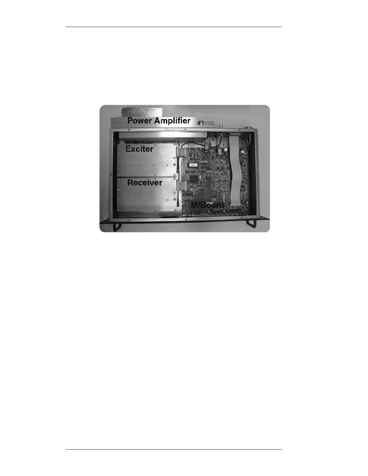
The internal design of the MX800 is of a modular nature allowing for simple
configuration and maintenance while ensuring minimal downtime. For
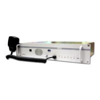
reference purposes, the top view of a typical MX800 with top cover removed
is shown in Figure 4-1 below. The standard unit without speaker and
microphone is illustrated.
Figure 4-1 MX800 Top View
4.1 Exciter Module
Refer:
Exciter Block Diagram: BD002
Exciter Circuit Diagram: CS002-1
TX VCO Circuit Diagram: CS004-1 (Bands A to Q)
CS011-1 (Bands R to X)
RF from the VCO on SKU-1 at a nominal level of +3dBm is applied to the
fractional-N synthesiser IC10 main divider input. This signal is compared
with the reference oscillator frequency and the correction voltage from the
synthesiser’s charge pump output is filtered then amplified by the non
inverting low noise op amp IC9A. This correction voltage is fed back to the
VCO to maintain loop lock as well as being fed to the Micro Controller via
SKD-14. A lock detect signal from IC10 is also fed to the Micro Controller
via SKD-16. The op amp uses a 25 volt power supply (generated on the
Micro Controller) so as to provide a wide tuning range voltage to the
frequency control varicaps located on the VCO board. Frequency
programming data for the exciter is sent to the synthesiser chip from the
Micro Controller via a serial data line on SKD-18 under the control of the
Clock (SKD-15) and Strobe (SKD-17) lines.