Power supplies AN4661
22/54 DocID027559 Rev 5
The following conditions must be respected:
• V
DD
should always be higher than V
CAP
to avoid a current injection between power
domains.
• If the time for V
CAP
to reach V12 minimum value is smaller than the time for V
DD
to
reach 1.7 V, then PA0 should be kept low to cover both conditions: until V
CAP
reaches
V12 minimum value and until V
DD
reaches 1.7 V.
• Otherwise, if the time for V
CAP
to reach V12 minimum value is smaller than the time for
V
DD
to reach 1.7 V, then PA0 could be asserted low externally.
• If V
CAP
goes below V12 minimum value and V
DD
is higher than 1.7 V, then PA0 must
be asserted low externally.
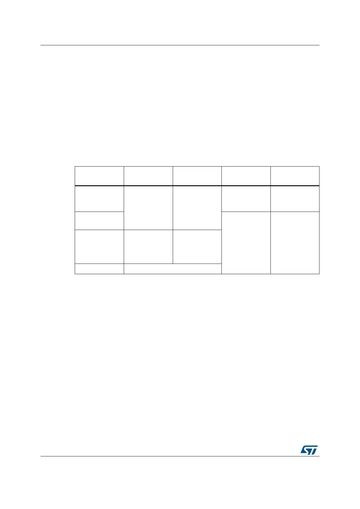
1.3.7 Regulator ON/OFF and internal reset ON/OFF availability
Table 1. Regulator ON/OFF and internal reset ON/OFF availability
Package Regulator ON Regulator OFF Internal reset ON
Internal reset
OFF
LQFP64
(1)
LQFP100
WLCSP100
(2)
1. Available only on the STM32F7x2xx devices.
2. Available only on the STM32F7x3xx devices.
Yes No
Yes No
LQFP144,
LQFP208
(3)
3. Not available on the STM32F72xxx/73xxx devices.
Yes
PDR_ON set to
V
DD
Yes
PDR_ON set to
V
SS
LQFP176,
WLCSP143
(4)
,
UFBGA176,
TFBGA216
(3)
4. Available only on the STM32F767xx/STM32F777xx devices.
Yes
BYPASS_REG set
to V
SS
Yes
BYPASS_REG set
to V
DD
WLCSP180 Yes
(5)
5. Available only on dedicated part numbers. Refer to ordering information section of the datasheet.
 Loading...


