DocID027559 Rev 5 31/54
AN4661 Debug management
53
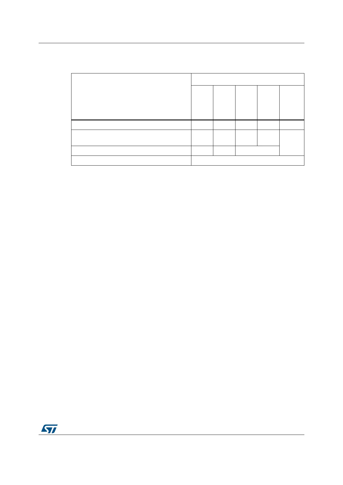
Table 5 shows the different possibilities to release some pins.
For more details on how to disable SWJ-DP port pins, please refer to RM0385 I/O pin
alternate function multiplexer and mapping section.
5.3.3 Internal pull-up and pull-down on JTAG pins
It is necessary to ensure that the JTAG input pins are not floating since they are directly
connected to flip-flops to control the debug mode features. A special care must be taken
with the SWCLK/TCK pin which is directly connected to the clock of some of these flip-flops.
To avoid any uncontrolled IO levels, the device embeds internal pull-ups and pull-downs on
the JTAG input pins:
• NJTRST: internal pull-up.
• JTDI: internal pull-up.
• JTMS/SWDIO: internal pull-up.
• TCK/SWCLK: internal pull-down.
Once a JTAG IO is released by the user software, the GPIO controller takes control again.
The reset states of the GPIO control registers put the I/Os in the equivalent state:
• NJTRST: AF input pull-up.
• JTDI: AF input pull-up.
• JTMS/SWDIO: AF input pull-up.
• JTCK/SWCLK: AF input pull-down.
• JTDO: AF output floating.
The software can then use these I/Os as standard GPIOs.
Note: The JTAG IEEE standard recommends to add pull-ups on TDI, TMS and nTRST but there is
no special recommendation for TCK. However, for JTCK, the device needs an integrated
pull-down.
Having embedded pull-ups and pull-downs removes the need to add external resistors.
Table 5. Flexible SWJ-DP assignment
Available debug ports
SWJ IO pin assigned
PA13 /
JTMS /
SWDIO
PA14 /
JTCK /
SWCL
K
PA15 /
JTDI
PB3 /
JTDO
PB4 /
NJTRST
Full SWJ (JTAG-DP + SW-DP) - reset state X X X X X
Full SWJ (JTAG-DP + SW-DP) but without
NJTRST
XXXX
-
JTAG-DP disabled and SW-DP enabled X X -
JTAG-DP disabled and SW-DP disabled Released
 Loading...


