Debug management AN4661
30/54 DocID027559 Rev 5
In the SWJ-DP, the two JTAG pins of the SW-DP are multiplexed with some of the five JTAG
pins of the JTAG-DP.
For more details on the SWJ debug port refer to RM0385 SWJ debug port section (serial
wire and JTAG).
5.3 Pinout and debug port pins
The STM32F7 Series devices are available in various packages with different numbers of
available pins. As a result, some functionality related to the pin availability (TPIU parallel
output interface) may differ between the packages.
5.3.1 SWJ debug port pins
Five pins are used as outputs from the STM32F7 Series for the SWJ-DP as alternate
functions of general-purpose I/Os. These pins are available on all packages.
5.3.2 Flexible SWJ-DP pin assignment
After RESET (SYSRESETn or PORESETn), all the five pins used for the SWJ-DP are
assigned as dedicated pins immediately usable by the debugger host (note that the trace
outputs are not assigned except if explicitly programmed by the debugger host).
However, the STM32F7 Series devices offer the possibility of disabling some or all of the
SWJ-DP ports and so, of releasing the associated pins for general-purpose IO (GPIO)
usage.
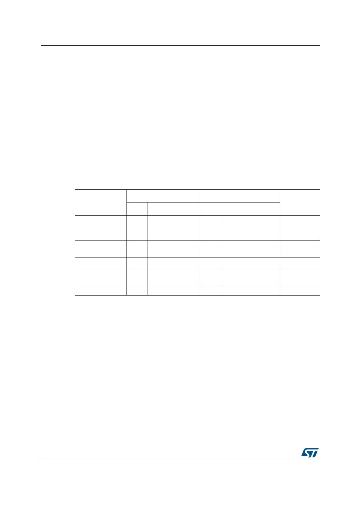
Table 4. SWJ debug port pins
SWJ-DP pin name
JTAG debug port SW debug port
Pin
assignment
Type Description Type Debug assignment
JTMS/SWDIO I
JTAG test mode
Selection
IO
Serial wire data
input/output
PA13
JTCK/SWCLK I JTAG test clock I Serial wire clock PA14
JTDI I JTAG test data input - - PA15
JTDO/TRACESWO O
JTAG test data
output
-
TRACESWO if async
trace is enabled
PB3
NJTRST I JTAG test nReset - - PB4
 Loading...


