DocID027559 Rev 5 49/54
AN4661 Recommended PCB routing guidelines for STM32F7 Series devices
53
8.5.2 WLCSP143 0.4 mm pitch design example
A better way to route this package and the fan-out signals is to use a through microvia
technology. Microvia will route out internal bumps to a buried layers inside the PCB. To
achieve this, the WLCSP package pads have to be connected to this internal layer through
microvia. In case of four layers PCB, the first layer is WLCSP component, the second layer
will be used as a signal layer, the third layer as the power and ground and the bottom layer
for a signal layout.
Figure 31 shows an example of the layout for four layers PCB.
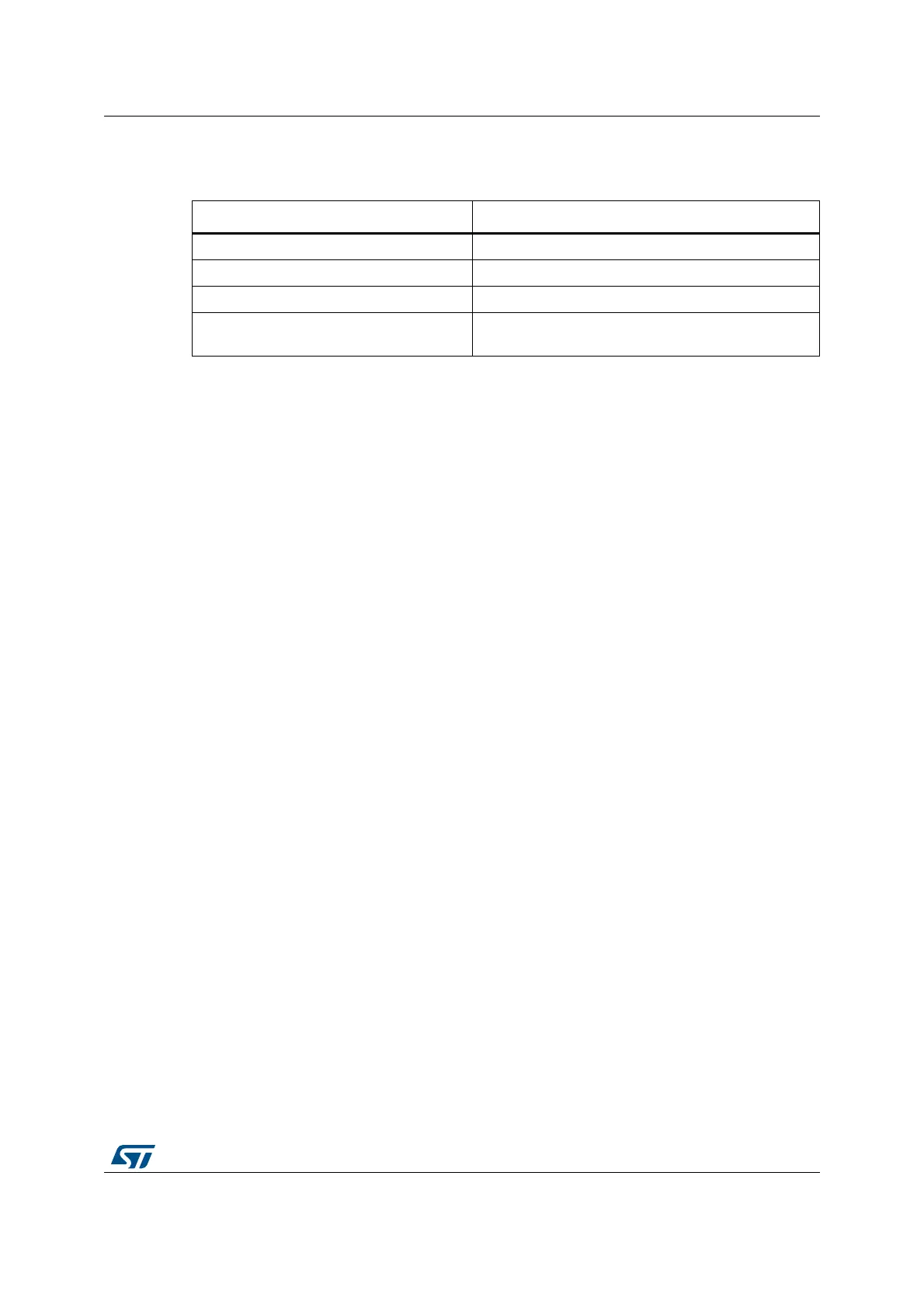
Table 10. Wafer level chip scale package information
Package information (mm) Design parameters (mm)
Bump pitch : 0.4 Microvia size : hole size ∅= 0.1, via land: 0.2
Bump size : 0.25 Trace width/space : 0.07/0.05 or 0.07/0.07
Number of rows/columns : 13x11 Bump pad size ∅= 0.26 max – 0.22 recommended
Non-solder mask defined via underbump
allowed
Solder mask opening bump ∅=0.3 min (for 0.26
diameter pad)
 Loading...


