DocID027559 Rev 5 43/54
AN4661 Recommended PCB routing guidelines for STM32F7 Series devices
53
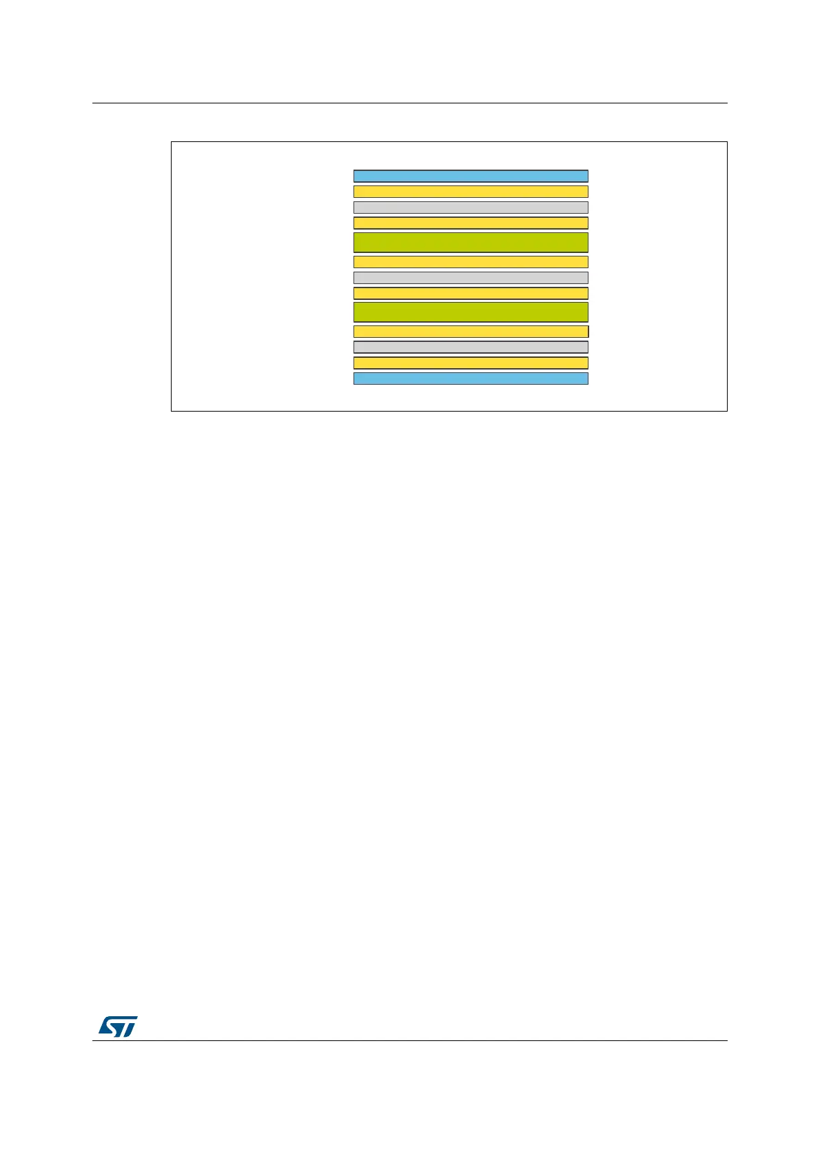
Figure 26. Six layer PCB stack-up example
8.2 Crystal oscillator
Use the application note: Oscillator design guide for STM8S, STM8A and STM32
microcontrollers (AN2867), for further guidance on how to layout and route crystal oscillator
circuits.
8.3 Power supply decoupling
An adequate power decoupling for STM32F7 Series is necessary to prevent an excessive
power noise and ground bounce noise. Please refer to
Section 1.2: Power supply scheme.
Figure 27 shows an example of placing bypass capacitors underneath STM32F7 Series
closer to pins and with less vias:
06Y9
6ROGHU0DVN
+LJK6SHHG6LJQDOV*1'
*1'3ODQH
3RZHU3ODQH
+LJK6SHHG6LJQDOV*1'
3UHSHJ
&RUH
3UHSHJ
6ROGHU0DVN
/D\HUB7RS
/D\HUB,QQHU
/D\HUB,QQHU
/D\HUB%RWWRP
3UHSHJ
/RZ6SHHG6LJQDOV
&RUH
*1'3ODQH
/D\HUB,QQHU
/D\HUB,QQHU
 Loading...


