To easily rework the ME910G1 it is recommended to consider on the application a 1.5 mm
placement inhibit area around the module.
It is also suggested, as common rule for an SMT component, to avoid having a mechanical
part of the application in direct contact with the module.
Note: In the customer application, the region in WIRING INHIBIT (see
figure above) must be clear from signal or ground paths.
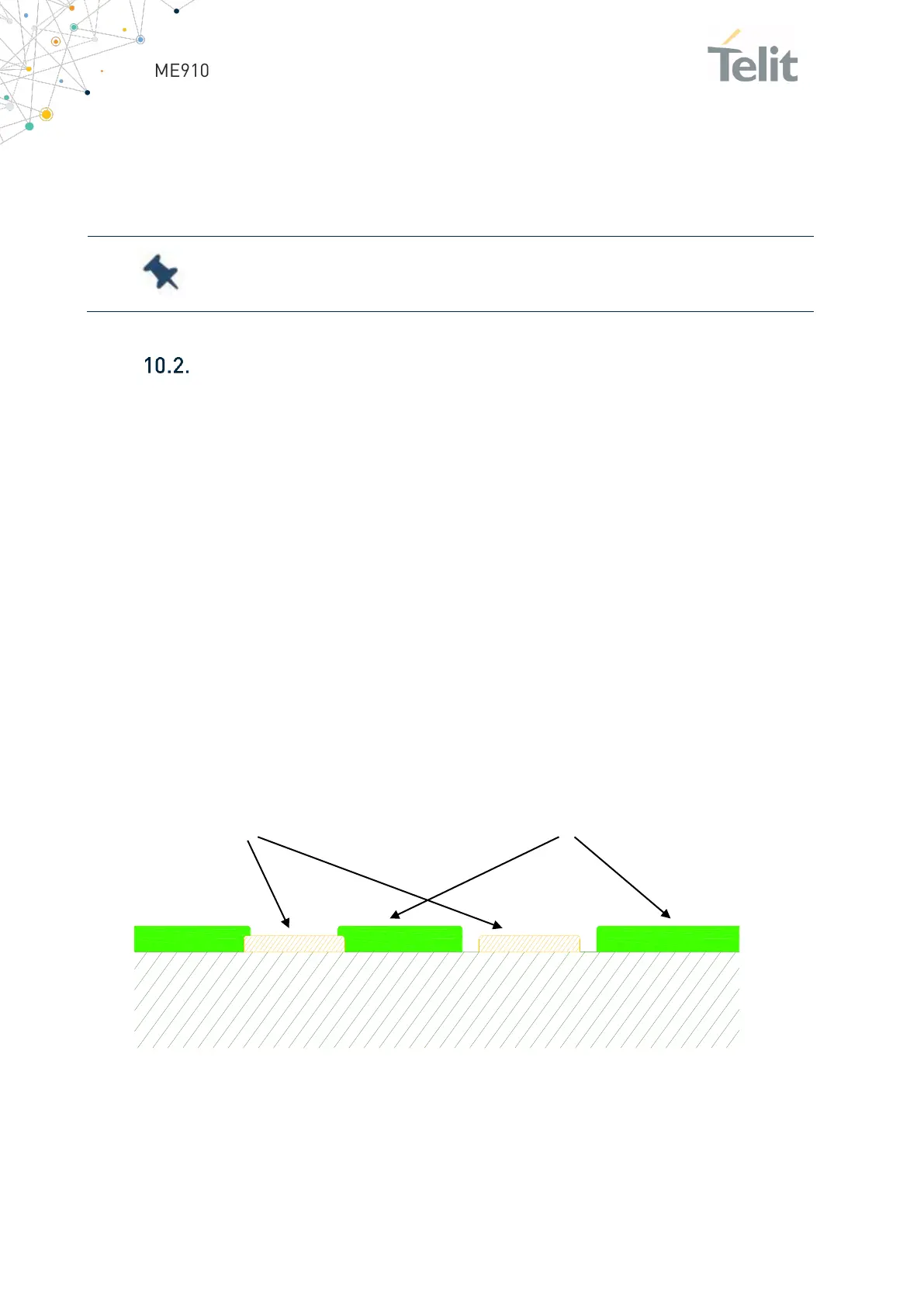
PCB Pad Design
In PCB design, solder pads can be defined as either Solder Mask Defined (SMD) or Non-
Solder Mask Defined (NSMD). The difference between these two solder mask pad
definitions is in the proximity of the solder mask to the metal pad. In SMD pads, the solder
mask opening is smaller than the metal pad and overlaps the metal on all sides. The
opening of the solder mask defines the solderable area of the pad. In NSMD pads, the
opening of the solder mask is larger than the metal pad and does not overlap the metal.
The metal edge defines the solderable area of the pad (see Figure below).
Since the metal etching process in PCB manufacture, has significantly tighter alignment
and etching tolerances than solder masking process alignment registration, which, a
more accurate solder pad land pattern can be obtained with NSMD pads. Also, with SMD
pads, the solder mask overlapping the metal pad introduces additional height above the
metal surface which may the adhesion and reliability of the solder joint. Non solder mask
defined (NSMD) type is recommended for the solder pads on the PCB.
Figure 28: PCB solder pad recommendations
 Loading...