www.ti.com
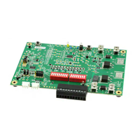
bq77910A EVM Circuit Description and Configuration
The user should note there are two limits implied by the absolute maximum cell-to-cell differential rating of
the part. One is the applied differential voltage, or 5V on any cell regardless of the other inputs. Note also
this is an applied voltage, not the voltage induced by the part during balancing, which may be higher. The
second voltage limit is the voltage to ground the cumulative voltage from summing the individual limits.
Since the input filter time constant is small, clamping the inputs to safe values may be required. While a
zener or TVS diode per cell may be a suitable way to protect the device in some applications, the EVM
provides patterns D12 to D18 to clamp the inputs for cells 10 to 4 to ground. The top cell input is clamped
(VC1 with D12 on the EVM), and cell 4's input, VC7 is clamped with D18 on the EVM since this input
showed more sensitivity than others in testing. For nominal transients, these clamps in conjunction with
the capacitors between cells should hold the inputs to safe values, however different or additional
clamping may be required in evaluation or the target application.
The EVM has resistor jumper positions and is populated to connect to the cells with N+1 wires where N is
the number of cells. R42 connects the high current BATT– connection to the lowest cell monitor point.
Similarly R59 connects cell 10 input to the high current path through R3. Additional resistor patterns R53
to R58 allow the same connections when the board is configured for other series cell counts. The board
may be configured to monitor the cell voltages directly at the cells (N+3 wires) by removing R42 and R59
or its equivalent.
When configuring the part for fewer than 10 cells, the unused inputs should not be left floating and must
be connected to avoid exceeding absolute maximums. The EVM provides patterns to allow flexible
connections. The unused pin group may be connected together on the EVM by shorting the capacitors
between them or shorting the appropriate resistor jumper positions R60 to R64. The unused pin group
then needs to be connected to a safe level, either to the top cell through one of the unused cell R
VCX
patterns or to the highest used VCx pin using the appropriate R61 to R65. When configuring for fewer
than 10 cells and using the cell simulator, be sure to remove components to avoid parallel paths. Due to
the flexibility allowed by the EVM for configuration it is recommended the evaluator study the schematic
before modifying the board to achieve their desired configuration. Table 9 shows possible configurations
for different cell counts assuming use of the cell simulator, retaining the N+1 wiring plan and adjusting the
transient protection. The board will operate at a lower cell count without the transient protection
adjustment, but the user should be sure they provide adequate protection for the IC in the evaluation and
system design to prevent damage. The table describes a change from the 10-cell default to one of the
other configurations, the users should check configurations if multiple changes are made. D12 is shown
removed in the table for less than 10 cells to avoid any possible leakage current or unexpected clamp
during evaluation.
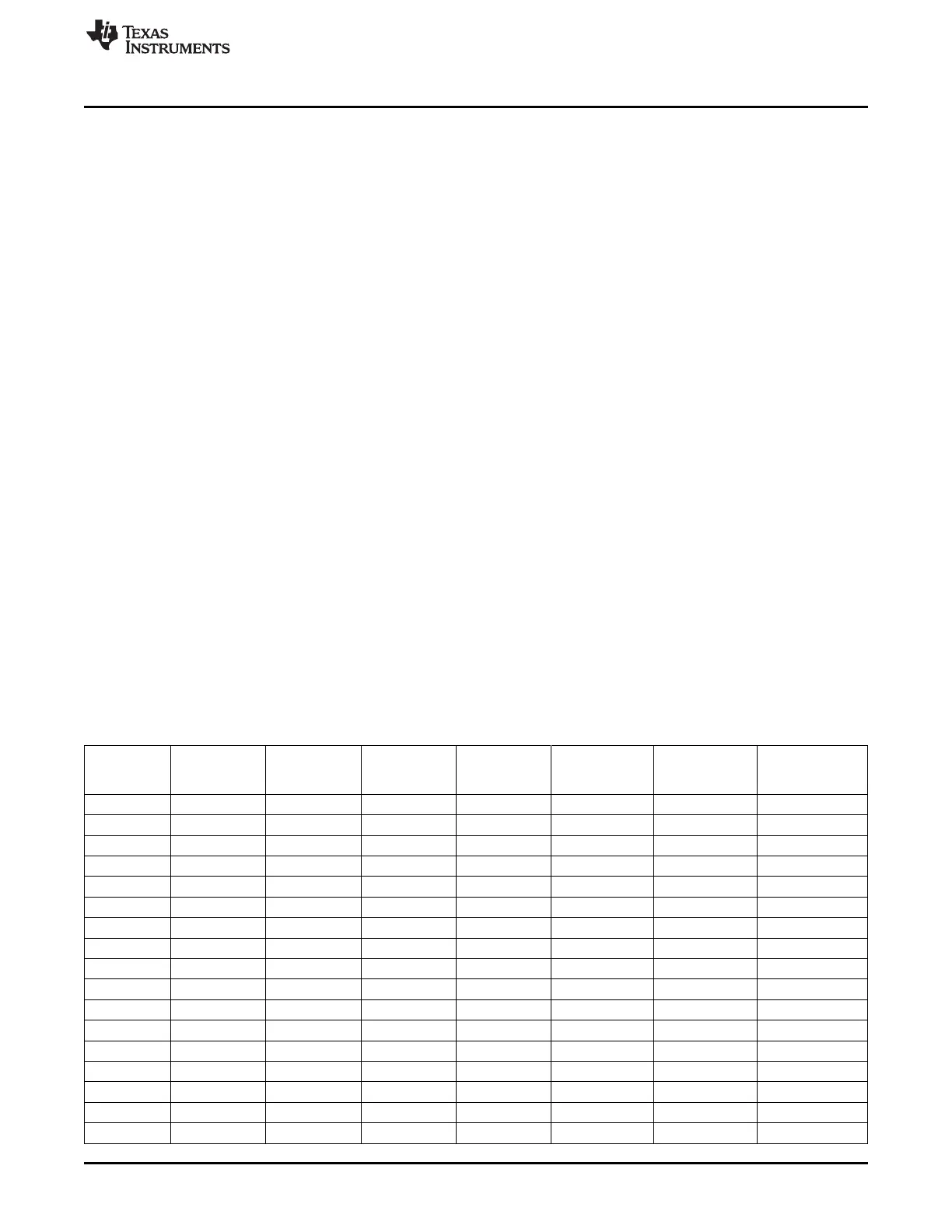
Table 9. Cell Count Component Configuration
Cell Count/
10 Cells
Reference 9 Cells 8 Cells 7 Cells 6 Cells 5 Cells 4 Cells
(Default)
Designator
C3 installed Remove installed installed installed installed installed
C5 installed installed Remove installed installed installed installed
C6 installed installed installed Remove installed installed installed
C7 installed installed installed installed Remove installed installed
C8 installed installed installed installed installed Remove installed
C9 installed installed installed installed installed installed Remove
D1 installed < 45V < 40V < 35V < 30V < 25V < 20V
D9 installed < 45V < 40V < 35V < 30V < 25V < 20V
D12 installed Remove Remove Remove Remove Remove Remove
D13 — < 45V — — — — —
D14 — — <40 V — — — —
D15 — — — <35V — — —
D16 — — — — < 30V — —
D17 — — — — — < 25V —
D18 installed installed installed installed installed installed installed
R7 installed Remove Remove Remove Remove Remove Remove
R11 installed installed Remove Remove Remove Remove Remove
19
SLUU855–February 2012 bq77910AEVM
Submit Documentation Feedback
Copyright © 2012, Texas Instruments Incorporated