www.ti.com
bq77910A EVM Circuit Description and Configuration
7.6 Filter Capacitors
The regulator filter capacitor C17 value of 4.7µF exceeds the minimum datasheet value of 1 μF. The 1-μF
DCAP and CCAP filter capacitors C21 and C26 are the data sheet recommended typical values.
7.7 FET Circuits
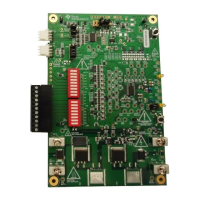
The circuit board has 5 TO-220 power FET patterns to allow flexibility in evaluation. By default the board
is populated for parallel FET operation. The Q3 discharge FET is mounted to a heatsink expecting high
discharge currents. The user should monitor temperature in their evaluation environment and provide
additional cooling if required. Q7 is the parallel charge FET. Anticipating a low charge current of up to a
couple amps, Q7 does not have a heatsink. The user should measure the device temperature in their
evaluation environment and provide heatsinking and cooling if required.
The Q4 pattern allows a FET to be installed instead of Q7 to provide series FET configuration. In this case
the pack negative would be the CHG– terminal. HS2 pattern is provided for Q4. If configured for series
FETs it is recommended to insulate DSG– to avoid erroneous connections. Patterns Q5 ane Q6 are in
parallel with Q3 and Q4 to provide for optional patterns, to allow parallel FET connection, to provide for a
large heatsink to be mounted to the FETs off the board edge if desired, or to provide connection points for
additional circuitry.
C34 and C35 provide a ESD path and high frequency bypass during switching of the discharge FET. Two
capacitors in series are used so that if one is shorted, the other still blocks DC signals. C36 and C37
provide a similar function for the charge FET or across both FETs in series configuration.
Several other components relate to the FET operation. R48 and R49 pull down the gate to source voltage
for the FETs to keep them off when the bq77910A is shut down. R41 is the discharge FET gate drive
resistor, 1k on the EVM. This value will adjust the turn off time of the discharge FET. Increasing the turn
off time will reduce the inductive transients during a protection event, but will increase heating in the
discharge FET. FET turn on is also affected, be sure to consider this if the system can turn on with load
applied. The 1k value may need to be adjusted for your application or other FETs, consult the FET vendor
data. R51 and C33 patterns provide locations to provide feedback to slow the discharge FET switching if
appropriate in your application. The charge FET typically can be allowed to switch faster due to lower
current. The value of R47 can be adjusted if desired.
When no FETs are desired, Q7 and Q3 can be shorted source to drain. Shorting the FETs is important in
this case both to provide a high current output path and to provide a proper reference for the DPCKN,
CPCKN and CCAP signals. Adjustments to the flag circuitry may also be desired in this configuration.
7.8 Detection Sensing
The device detects load presence with the DPCKN pin. This is connected to the discharge negative signal
DSG– with R45. The 100 Ω value is the datasheet recommended typical R
DPCKN
and provides some
isolation of the pin from load transients. C29 provides some filtering to avoid transients pushing DPCKN
above its absolute max. D7 is an optional diode to limit the DPCKN voltage to the BAT pin clamp if
required, in testing it has not appeared necessary. R46 is the R
LDRM_DET
resistor in the datasheet. This
resistor discharges the load capacitance and in series FET configuration pulls down CPCKN to allow turn
on of the CHG output. Note that this resistor provides an un-switched load and should not be made too
small. R46 might be removed in parallel FET configurations to reduce the battery drain during continued
loads after protection since the device has a weak internal pull down on DPCKN.
CPCKN is the charge negative sense which is used by the device to sense the charge FET source
voltage. It is also the negative power supply for the CHG output driver. R40 is the datasheet R
CPCKN
and is
the typical recommended value. C30 is an optional pattern for filtering if desired. D8 limits the voltage
across BAT to CPCKN during transients or situations when the applied charger voltage exceeds the
device absolute maximum. D8 also functions in the series FET configuration to prevent CPCKN from
significantly exceeding BAT.
21
SLUU855–February 2012 bq77910AEVM
Submit Documentation Feedback
Copyright © 2012, Texas Instruments Incorporated
