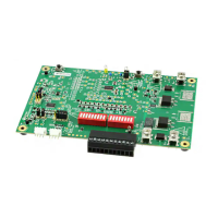
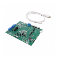
bq77910A Circuit Module and Interfaces
www.ti.com
2.2 Signal Descriptions
Signals available on the EVM are described in this section. For details on the location and connector
types, refer to the physical construction section. High current signals can be connected at either the
terminal block or banana jack. Refer to the physical construction section for identification.
Cell connections are described in Table 2. The default board assembly supports only 5 cells, so the upper
cell connections are not used. CELL0 and CELL5 are connected to the high current paths on the board
through 0-Ω resistors. This allows operation of the resistive cell simulator without external connections. If
the on-board resistors are removed, connections must be made off the board. Refer to the physical
construction section for resistor identification. Cell connection sequence is described in Section 3.6.
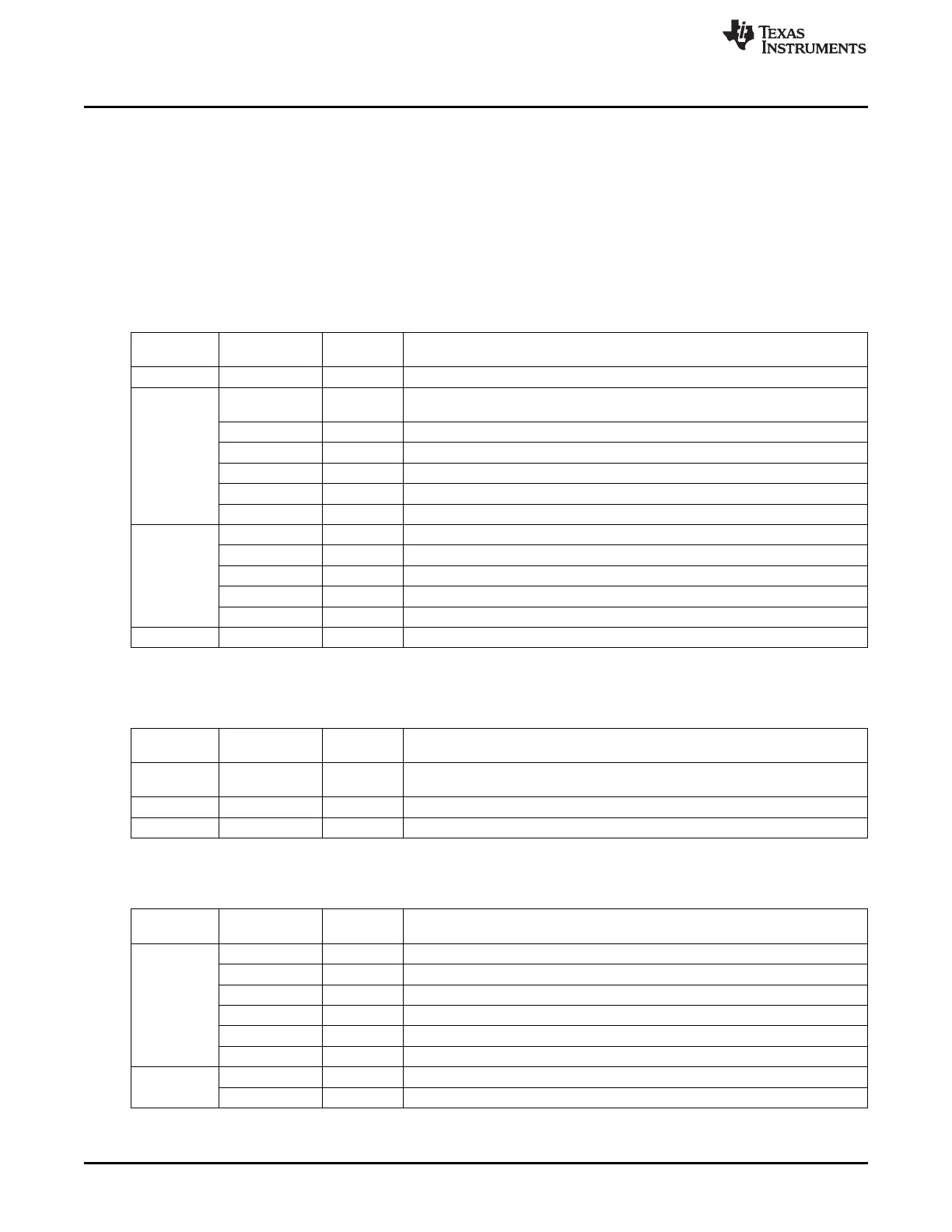
Table 2. Cell Connections
Reference
Pin Number Signal Description
Designator
J13, J15 All BATT– Negative electrode of first (bottom) cell, high current connection
J5 6 CELL0 Negative electrode of first (bottom) cell, optional separate monitor connection to
cell
5 CELL1 Positive electrode of first (bottom) cell
4 CELL2 Positive electrode of second cell
3 CELL3 Positive electrode of third cell
2 CELL4 Positive electrode of fourth cell
1 CELL5 Positive electrode of fifth cell,
J4 5 CELL6 Positive electrode of sixth cell
4 CELL7 Positive electrode of seventh cell
3 CELL8 Positive electrode of eighth cell
2 CELL9 Positive electrode of ninth cell
1 CELL10 Positive electrode of tenth cell, optional separate monitor connection to cell
J10, J11 All PACK+ Most positive cell output, high current connection, shared with PACK+
Load connections are described in Table 3.
Table 3. PACK Connections
Reference Pin Number
Signal Description
Designator
J10, J11 All PACK+ Positive output of evaluation board, shared with the battery high current
connection
J12, J14 All DSG– Negative output of evaluation board for discharge
J16, J17 All CHG– Negative input to evaluation board for charge
Programming signals are described in Table 4. J3 signals are 3.3V logic level.
Table 4. Programming Interface Connections
Reference Pin Number
Signal Description
Designator
J3 1, 2, 5, 7, 8 Not used
3 PGM Control signal for EEPROM programming voltage.
4 ZD Control signal for device ZEDE
6 GND Signal reference for the IC
9 ECLK Serial interface clock connection
10 EDATA Serial interface data connection
J2 1 14V Regulated 14V input for IC programming
2 GND Signal reference for the IC
4
bq77910AEVM SLUU855–February 2012
Submit Documentation Feedback
Copyright © 2012, Texas Instruments Incorporated