66
66
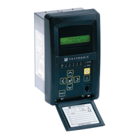
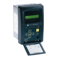
NV10P - Manual - 01 - 2015
CHARACTERISTICS
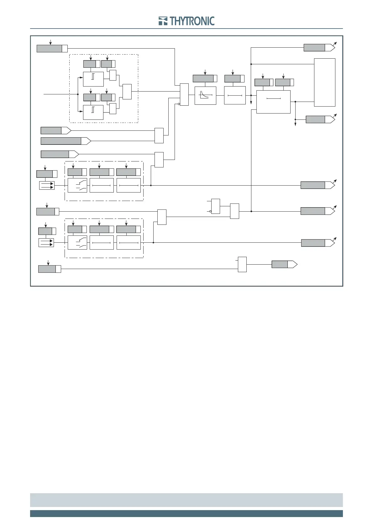
For every of the two thresholds the logic block can be set.
Logical block (Block1)
If the UE>BLK1 and/or UE>>BLK1 enabling parameters are set to ON and a binary input is de-
signed for logical block (Block1), the protection is blocked off whenever the given input is active.
The trip timer is held in reset condition, so the operate time counting starts when the input block
goes down.
[1]
The enabling parameters are available inside the Set \ Profi le A(or B) \ Residual over-
voltage - 59N \ UE> Element (UE>> Element) \ Setpoints menus, while the Block1 function must be
assigned to the selected binary input inside the Set \ Inputs \ Binary input IN1(2) menus (IN1 or IN2
matching).
All the named parameters can be set separately for Profi le A and Profi le B).
Note 1 The exhaustive treatment of the logical block (Block 1) function may be found in the “Logic Block” paragraph inside CONTROL AND MONITOR-
ING section.
Logic diagram concerning the first threshold (UE>) of the residual overvoltage element - 59N
Fun-F59N_S1.ai
≥1
U
E
> Inhibition
(ON≡
Inhibit
)
&
U
E
> Curve
0T
RESET
t
UE>
0T
TRIPPING MATRIX
(LED+RELAYS)
t
UE>def
t
UE>inv
Start U
E
>
U
E
>ST-K
U
E
>ST-L
Start U
E
>
Trip U
E
>
U
E
>TR-K
U
E
>TR-L
Trip U
E
>
Trip U
E
>
BF Enable (ON≡Enable)
UE>BF
towards BF logic
&
Block1 U
E
>
74VT ext.
U
E
> BF
&
&
&
Enable (ON≡Enable)
Block1 input (ON≡Block)
Block1
Block1
Binary input INx
T0
Logic
INx
t
ON
INx
t
ON
INx
t
OFF
T0
n.o.
n.c.
INx
t
OFF
74VText.
Binary input INx
T0
Logic
INx
t
ON
INx
t
ON
INx
t
OFF
T0
n.o.
n.c.
INx
t
OFF
t
UE>RES
T0
t
UE>RES
ON≡Enable UE> residual overvoltage element
UE> Enable
U
E
U
E
>def
U
E
>inv
≥1
&
State
U
E
≥
U
E
>def
U
E
≥
U
E
>inv
&
State
UE>BLK1
≥1
(1≡DDI closed)
DDI state
(1≡upstream)
UE>>disbyCB_OPEN