Hardware User Guide
1-12 Xilinx Development System
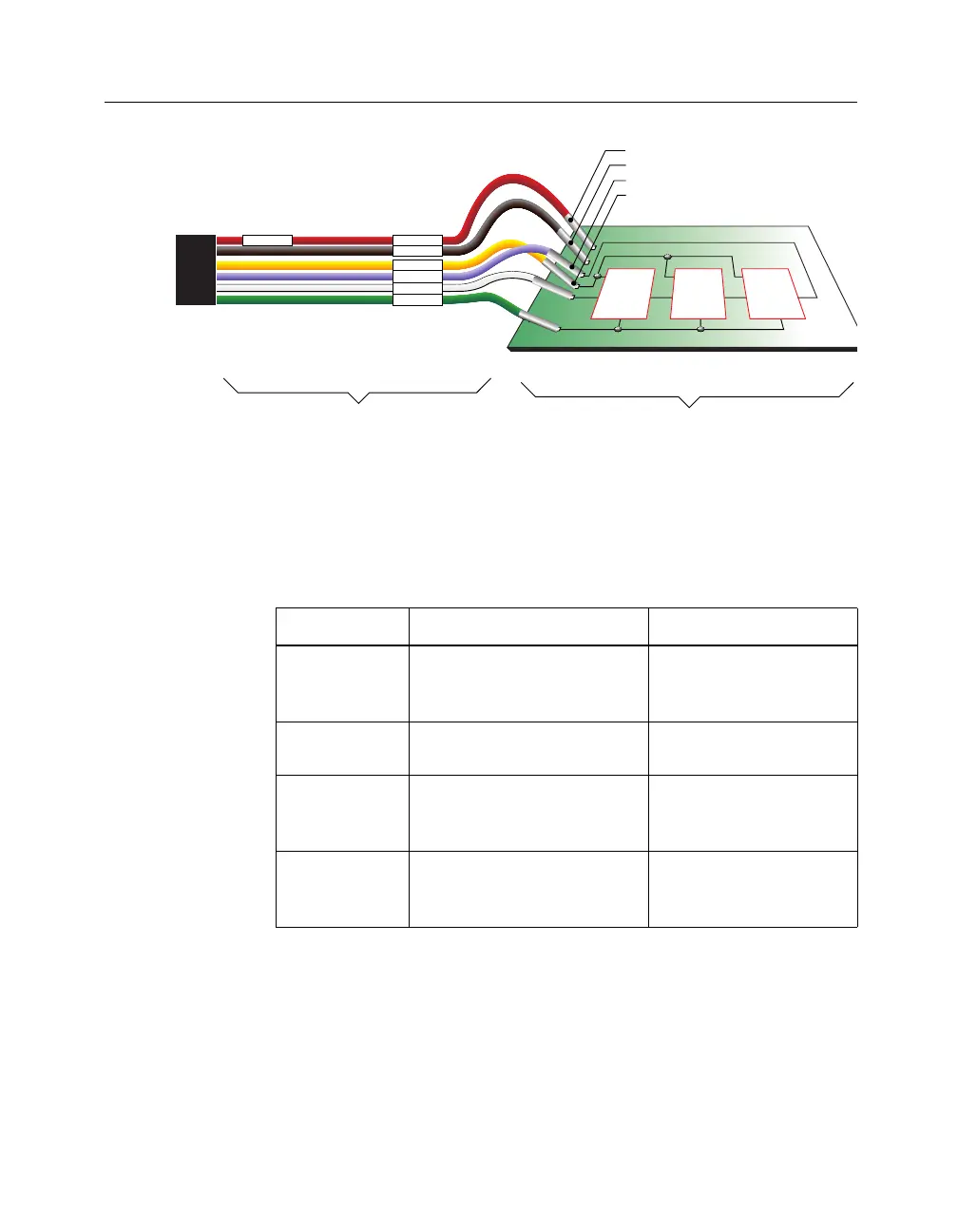
Figure 1-6 Parallel Cable III Connections to CPLD Device
The following table describes the pin functions and connections for
configuring CPLDs with the Parallel Cable III.
Table 1-3 Parallel Cable III CPLD Pin Connections
Name Function Connections
VCC Power – Supplies VCC (5
V, 10 mA, typically) to the
cable.
To target system VCC
GND Ground – Supplies ground
reference to the cable.
To target system
ground
TCK Test Clock – Drives the test
logic for all devices on a
JTAG chain.
Connect to system TCK
pin.
TDO Test Data Output – data
from the target system is
read at this pin.
Connect to system
TDO pin.
JTAG Flying Lead Connector
Target System
X83
TMS
TDI TDO
TCK
TMS
TDI TDO
TCK
TMS
TDI TDO
TCK
VCC
GND
TMS
TCK
JTAG
TMS
TDI
TDO
TDI
TCK
TDO
GND
VCC