Hardware User Guide
1-20 Xilinx Development System
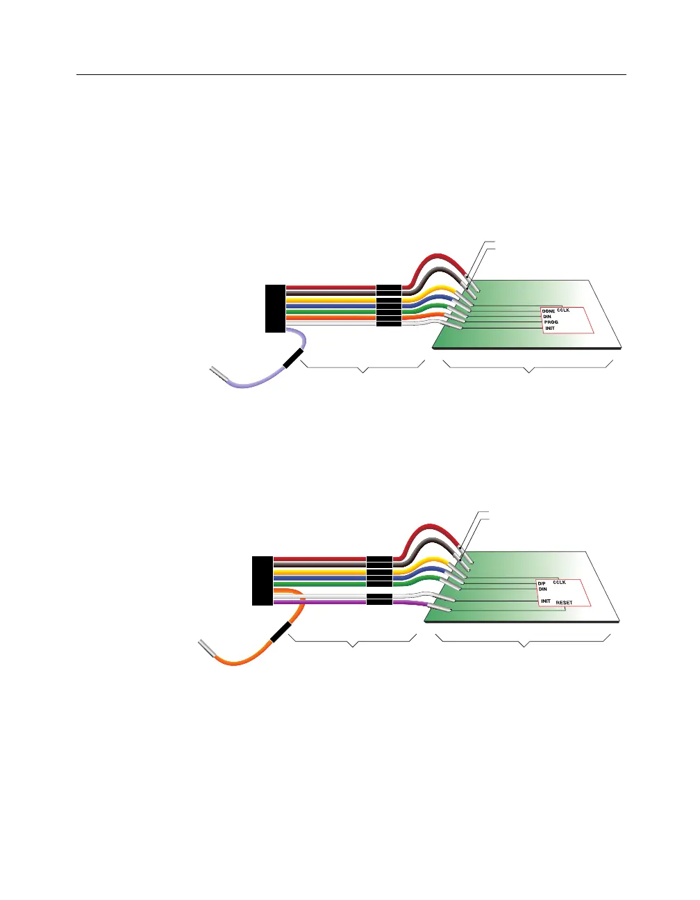
The following figures show which pins to connect, depending on
your chosen FPGA device. For descriptions of each pin, see Table 3-
6and Table 3-7 of the “FPGA Design Demonstration Board” chapter.
Use Header 1 (see Figure 1-9) to connect the XChecker Cable to the
target system for configuring FPGAs. When configuring XC4000
FPGAs,theRST(Reset)wireisnotusedasshowninthefollowing
figure.
Figure 1-11 XChecker Connections to XC4000 Device
To configure XC3000 FPGAs, the PROG wire is not used. This is
shown in the following figure. In both cases, the FPGA must be in the
Serial Slave Mode.
Figure 1-12 XChecker Connections to XC3000 Device
Pin Connection Considerations
The following adjustments will make the process of connecting and
downloading easier.
XChecker with Header 1
Target System
X8323
CCLK
GND
VCC
INIT
RST
DONE
DIN
PROG
INIT
XC4000 FPGA in Slave Serial Mode
Not Used
VCC
GND
PROG
CCLK
D/P
DIN
XChecker with Header 1
Target System
X8324
CCLK
GND
VCC
INIT
PROG
D/P
DIN
INIT
XC3000 FPGA in Slave Serial Mode
Not Used
RESET
VCC
GND
RST
CCLK
D/P
DIN