FPGA Design Demonstration Board
Hardware User Guide 3-17
The D/P wire from the FPGA header on the Parallel Cable III is
connected to J2-9 DONE pin.
Jumper J7 and Tiepoints J10 (1-3)
Jumper J7 allows the XChecker signal RST on J2-17 to drive the reset
line on the demonstration board. Tiepoint pins jumper the following
XChecker signals into the circuit. Tiepoint J10-1 connects to TRIG on
J2-6; Tiepoint J10-2 connects to CLK1 on J2-16; and, Tiepoint J10-3
connects to CLK0 on J2-18. See the preceding table for more details on
the cable and pin connections.
Serial PROM Socket (U2)
This serial PROM configures the XC4003E or the XC4003E and
XC3020A connected in a daisy chain. The configuration mode must
be in the master serial mode to configure from the serial PROM.
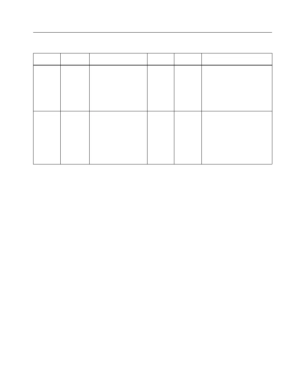
J2-15 INIT Goes Low if CRC
error occurs during
configuration.
Connects to
XC4003E INIT pin
41.
J2-16 CLK1 A system clock input to
XChecker Cable to be
controlled and output on
CLK0.
Connects to tiepoint J10-
2.
J2-17 RST Connects to jumper
J7. If connected,
allows XChecker
Cable to provide a
Resetinput(sameas
pressing the Reset
button).
J2-18 CLK0 A system clock output
controlled by XChecker
Cable. Used to single-
step or burst clocks to
the XC4003E.
Connects to tiepoint J10-
3.
a. Denotes pins supported by the Parallel Cable III
b. No pin connection
Table 3-6 XChecker/Parallel Cable III Connector J2
Pin Name Function Pin Name Function