FPGA Design Demonstration Board
Hardware User Guide 3-25
N = approximately 0.35 for TTl threshold
= approximately 0.75 for CMOS threshold
when the FPGA allows each capacitor to discharge during the oppo-
site timing phase.
Mode Switch Settings
This section describes the SW1 and SW2 switch settings for config-
uring the XC3020A and XC4003E devices.
• From the XChecker/Parallel Cable III
• From the serial PROM (single program)
• From the serial PROM (multiple program)
• In a daisy chain
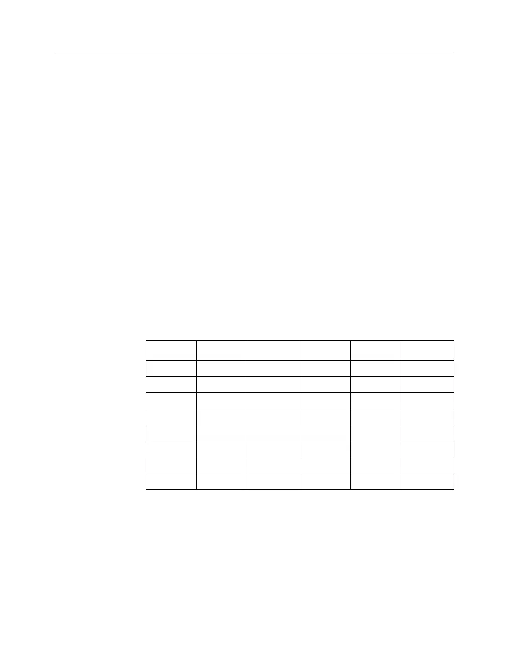
The following table lists the names and positions of the SW1 and SW2
switches for configuring the XC3020A FPGA from the XChecker or
Parallel Cable III.
Table 3-8 Configuring the XC3020A from the XChecker/Parallel
Cable III
Switch Name Position Switch Name Position
SW1–1 INP X SW2–1 PWR X
SW1–2 MPE OFF SW2–2 MPE X
SW1–3 SPE OFF SW2–3 SPE X
SW1–4 M0 ON SW2–4 M0 X
SW1–5 M1 ON SW2–5 M1 X
SW1–6 M2 ON SW2–6 M2 X
SW1–7 MCLK OFF SW2–7 RST
SW1–8 DOUT OFF SW2–8 INIT OFF
X indicates don‘t care