FPGA Design Demonstration Board
Hardware User Guide 3-21
To configure from the onboard serial PROM, these switches must be
off. This places the FPGA in master serial mode.
MCLK-Master Clock (SW1-7)
When this switch is on, it connects the XC4003E configuration clock
(pin 73) to the configuration clock on the XC3020A (pin 60). This
connection is used to configure FPGAs in a daisy chain with the
XC4003E at the head.
DOUT-Data Out (SW1–8)
When this switch is on, it connects the XC4003E data out line (pin 72)
to the data in line of the XC3020A. This connection configures FPGAs
in a daisy chain with the XC4003E at the head.
Note MCLKandDOUTshouldonlybeusedtoconfiguretheFPGAs
in a daisy chain.
XChecker/Parallel Cable III Connector J1
The following table describes the pins and functions of the
XChecker/Parallel Cable III J1 connector.
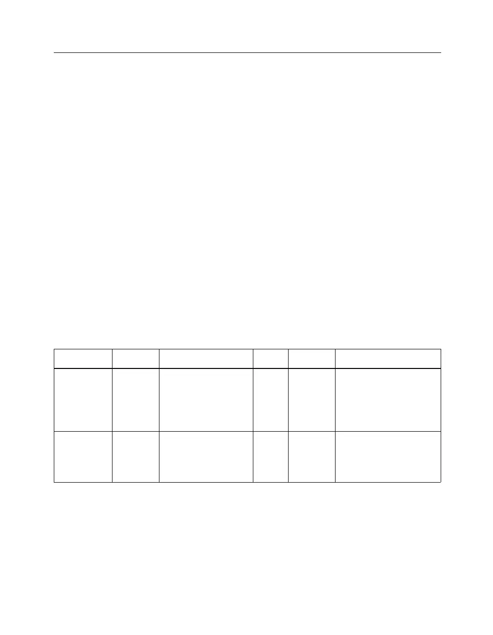
Table 3-7 XChecker/Parallel Cable III Connector J1
Pin Name Function Pin Name Function
J1–1
a
VCC Supplies +5 V to the
XChecker Cable.
J1–2 RT Allows XChecker
Cable to trigger a read-
back of the XC3020A.
Connects to XC3020A
pin 26.
J1–3
a
GND Supplies ground
reference to
XChecker Cable.
J1–4 RD Used by XChecker
Cable for readback
data. Connects to
XC3020A pin 25.