Cable Hardware
Hardware User Guide 1-19
Configuring FPGAs With the XChecker Cable
This section details the connections needed to configure FPGAs with
the XChecker Cable.
Note If you are using the Xilinx FPGA Design Demonstration Board,
see the “Demonstration Board Operation” section of the “FPGA
Design Demonstration Board” chapter for specific configuration
information.
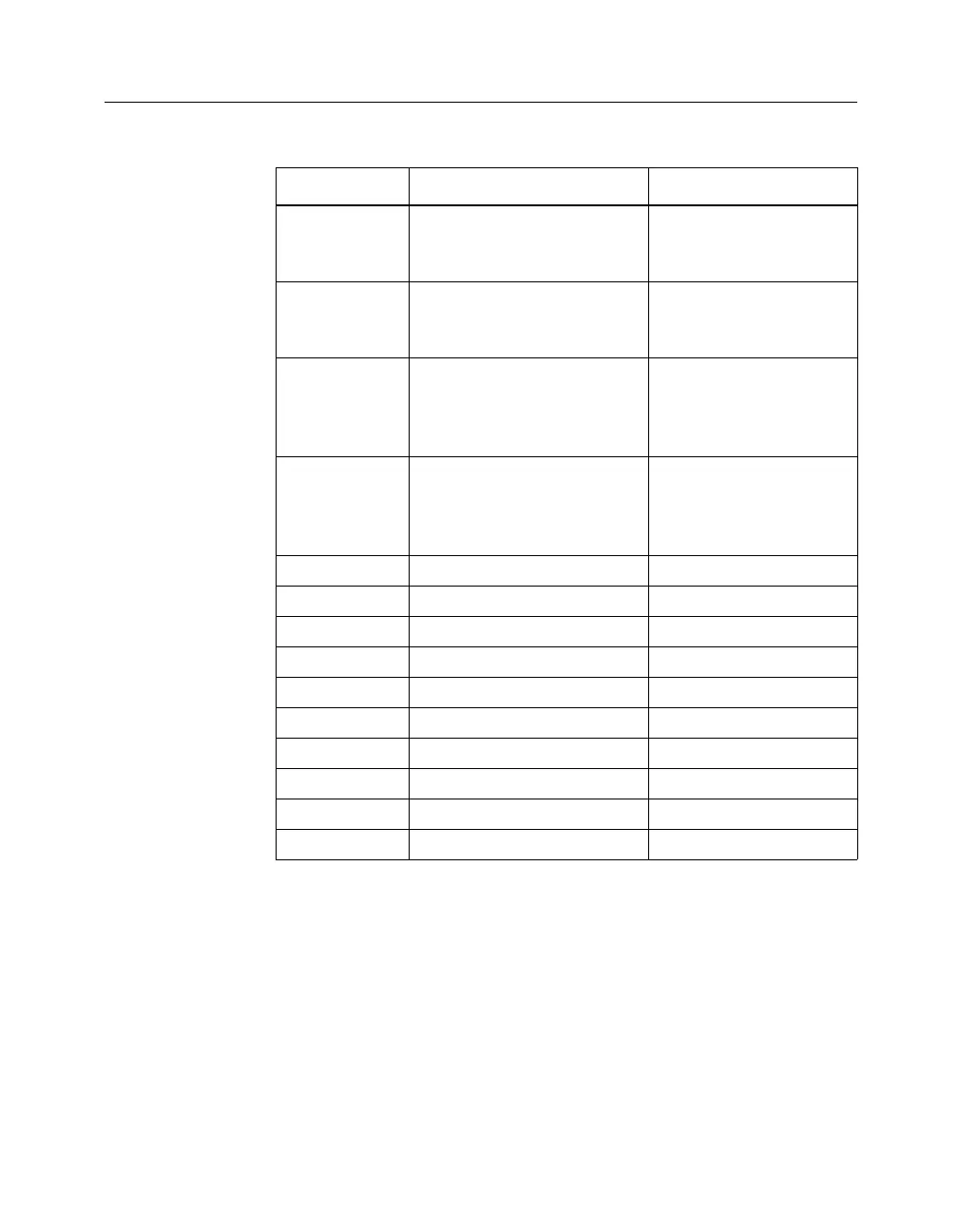
RD (TDO) Read Data – Reads back
data from the target
system is read at this pin.
Connect to system
TDO pin.
TDI Test Data In – this signal is
used to transmit serial test
instructions and data.
Connect to system TDI
pin.
TCK Test Clock – this clock
drives the test logic for all
devices on boundary-scan
chain.
Connect to system TCK
pin.
TMS Test Mode Select – this
signal is decoded by the
TAP controller to control
test operations.
ConnecttosystemTMS
pin.
CLKI Not used. Unconnected.
CLKO Not used. Unconnected.
CCLK Not used. Unconnected.
D/P Not used. Unconnected.
DIN Not used. Unconnected.
PROG Not used. Unconnected.
INIT Not used. Unconnected.
RST Not used. Unconnected.
RT Not used. Unconnected.
TRIG Not used. Unconnected.
Table 1-5 XChecker Cable Pin Connections for CPLDs
Name Function Connections