FPGA Design Demonstration Board
Hardware User Guide 3-3
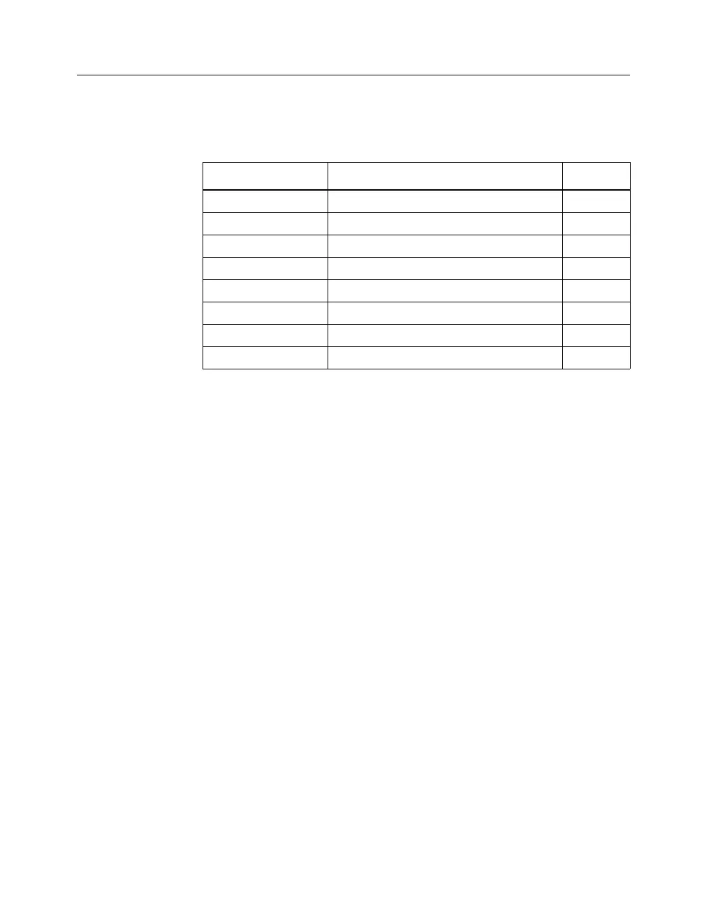
• Total of three 8-pin DIP switches to set up the XC4000 and
XC3000 FPGAs, as shown in the following table.
• 16 I/O lines that connect the two FPGAs
• An external relaxation oscillator circuit available to the user for
the XC3000
• The XC4000 OSC4 library symbol, which uses pin 19 of the
XC4003E to drive the XC3000 TCLKIN on pin 11 of the XC3020A
• TheXC4000OSC4,usespin13todrivetheXC3000alternate
clock buffer (BCLKIN) on pin 43
• Eight general purpose input switches to provide logic inputs to
the FPGAs
• Program, Reset, and Spare Active Low push-button switches,
which are common to both FPGAs
• An XC3000A display for the XC3000 device. The display uses
eight LED bars in one row and one 7-segment LED, as shown in
the following figure.
• An XC4000A display for the XC4000 device. The display uses
eight LED bars in one row and two 7-segment LEDs, as shown in
the following figure.
• Space for an optional +5 V regulator for battery operation
• Space for an optional crystal oscillator
• Headers for FPGA probe points
Table 3-1 DIP Switch Configuration
XC3000 SW1 XC4000 SW2 Switch
INP 1 PWR
MPE MPE (multiple configurations) 2
SPE SPE (single configuration) 3
M0 M0 4
M1 M1 5
M2 M2 6
MCLK RST 7
DOUT INIT 8