Hardware User Guide
3-8 Xilinx Development System
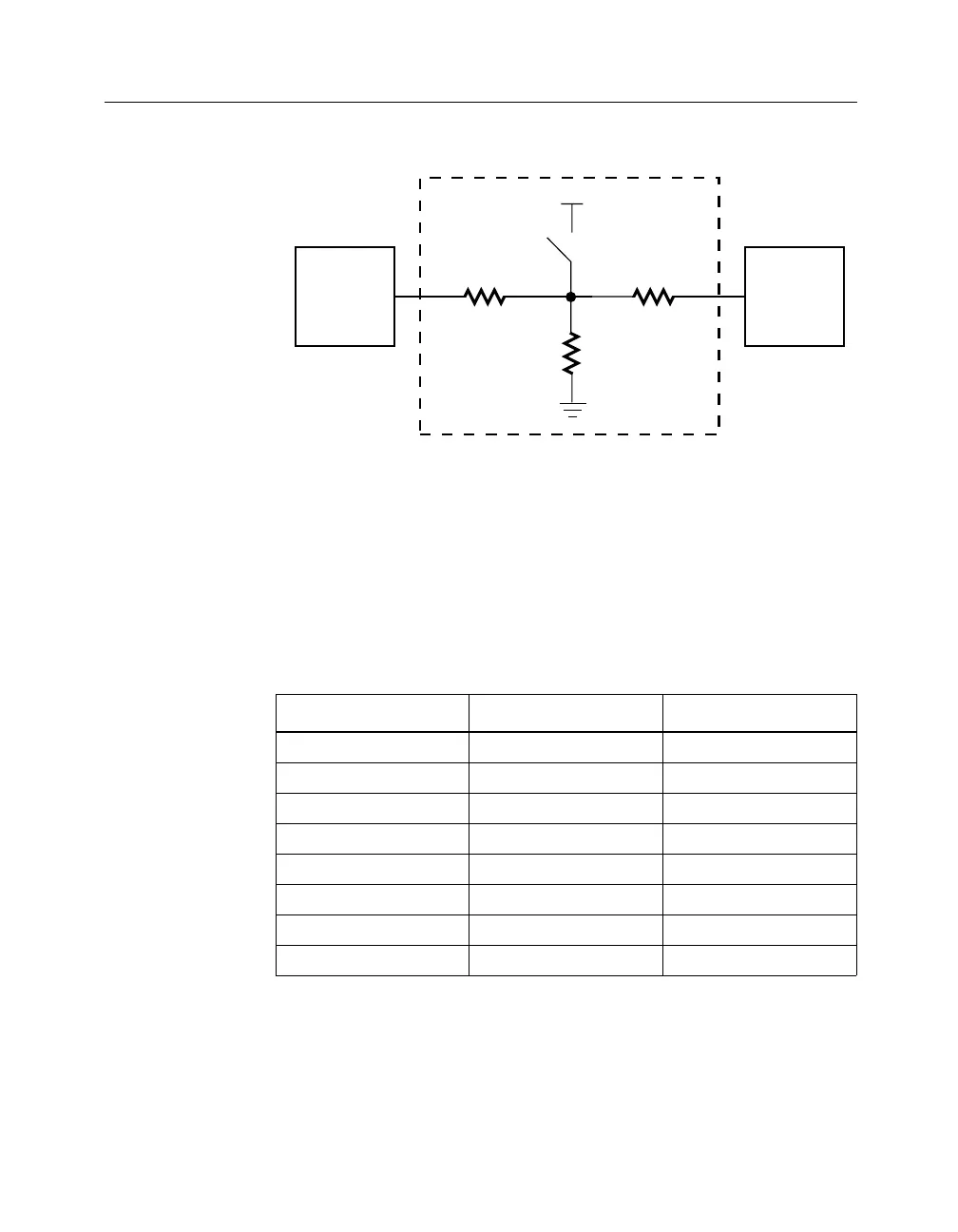
Figure 3-4 FPGA Demonstration Board General-Purpose Switch
The FPGA pins connected to this switch are intended for use as
inputs. However, each FPGA pin has a 1 kilohm resistor that isolates
it from the switch, so it is possible to define the pins as outputs. You
can also drive the pins from an external source by connecting that
signal to the FPGA probe point header. The following table lists the
FPGA pin connections.
Table 3-2 Input Switch Pin Connections
Switch XC3020A XC4003E
SW3–1 11 19
SW3–2 13 20
SW3–3 15 23
SW3–4 17 24
SW3–5 19 25
SW3–6 21 26
SW3–7 23 27
SW3–8 24 28
X4744
1K
XC3020A
1K
4.7K
SW3-n
+5V
XC4003E