ZC702 Board User Guide www.xilinx.com 18
UG850 (v1.7) March 27, 2019
Feature Descriptions
I/O Voltage Rails
There are four PL I/O banks available on the XC7Z020 SoC. The voltages applied to the
XC7Z020 SoC I/O banks used by the ZC702 board are listed in Table 1-3.
DDR3 Component Memory
[Figure 1-2, callout 2]
The 1 GB, 32-bit wide DDR3 memory system is comprised of four SDRAMs at U66–U69. This
memory system is connected to the XC7Z020 SoC processing system (PS) memory interface
bank 502.
Component Memory Details
• Part number: MT41J256M8HX-15E (Micron Technology)
• Configuration: 2Gb: 256 Mb x 8
• Supply voltage: 1.5V
• Datapath width: 32 bits
• Data rate: Up to 1,333 MT/s
The ZC702 XC7Z020 SoC PS DDR bank 502 interface performance is documented in the
Zynq-7000 SoC (Z-7007S, Z-7012S, Z-7014S, Z-7010, Z-7015, and Z-7020): DC and AC
Switching Characteristics (DS187) data sheet [Ref 3].
The DDR3 0.75V V
TT
termination voltage is sourced from linear regulator U22.
The connections between the DDR3 component memory and XC7Z045 SoC bank 502 are
listed in Table 1-4.
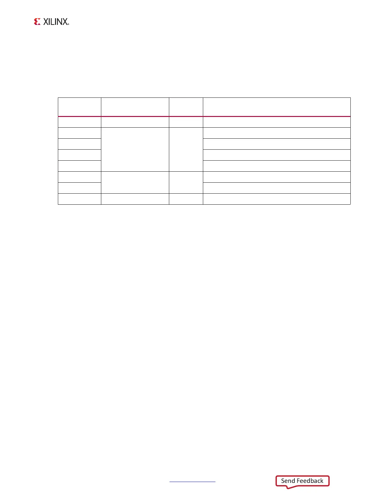
Table 1-3: I/O Voltage Rails
XC7Z020 (U1)
Bank
Net Name Voltage Connected To
PL Bank 0 VCC2V5_PL 2.5V SoC Configuration Bank 0
PL Bank 13
VADJ
(1)
2.5V
FMC2, GPIO, PL_PJTAG, IIC_MAIN
PL Bank 33 FMC2, HDMI Codec
PL Bank 34 FMC1, HDMI Codec
PL Bank 35 FMC1, HDMI Codec, XADC_GPIO, GPIO
PS Bank 500
VCCMIO_PS 1.8V
Quad-SPI flash memory, misc
PS Bank 501 Ethernet PHY, USB ULPI Transceiver, SDIO, CAN
PS Bank 502 VCC1V5_PS 1.5V PS_DDR3 MEM
Notes:
1. The ZC702 board is shipped with V
ADJ
set to 2.5V.