ZC702 Board User Guide www.xilinx.com 31
UG850 (v1.7) March 27, 2019
Feature Descriptions
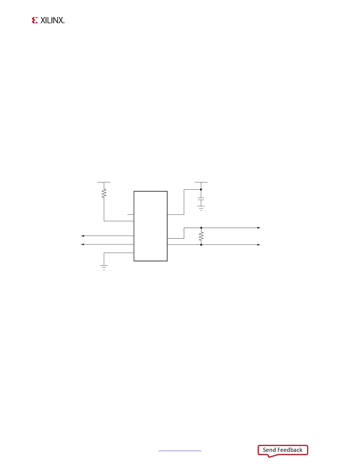
Programmable User Clock
[Figure 1-2, callout 8]
The ZC702 board has a programmable low-jitter 3.3V LVDS differential oscillator (U28)
connected to the MRCC inputs of bank 13. This USRCLK_P and USRCLK_N clock signal pair
is connected to XC7Z020 SoC U1 pins Y9 and Y8 respectively. On power-up the user clock
defaults to an output frequency of 156.250 MHz. User applications can change the output
frequency within the range of 10 MHz to 810 MHz through an I2C interface. Power cycling
the ZC702 board reverts the user clock to the default frequency of 156.250 MHz.
• Programmable Oscillator: Silicon Labs Si570BAB0000544DG (10 MHz–810 MHz)
• LVDS Differential Output
The user clock circuit is shown in Figure 1-12.
The Silicon Labs Si570 data sheet is available on the Silicon Labs website [Ref 19].
Processing System Clock Source
[Figure 1-2, callout 8]
The Processing System (PS) clock source is a 1.8V LVCMOS single-ended fixed
33.33333 MHz oscillator at U65. It is wired to PS bank 500, pin F7 (PS_CLK), on the XC7Z020
SoC.
• Oscillator: SiTime SiT8103AC-23-18E-33.33333 (33.3 MHz)
• Frequency Tolerance: 50 ppm
• Single-ended output
X-Ref Target - Figure 1-12
Figure 1-12: User Clock Source
UG850_c1_12_030513
GND
VCC3V3
1
2
3
8
7
6
U28
R20
4.7KΩ 5%
C216
0.01 μF 25V
X7R
4
5
GND
VCC3V3
Si570
Programmable
Oscillator
NC
OE
GND
SCL
SDA
VDD
CLK-
CLK+
R417
100Ω 1%
USRCLK SDA
USR CLK SCL
USRCLK N
USRCLK P