ZC702 Board User Guide www.xilinx.com 27
UG850 (v1.7) March 27, 2019
Feature Descriptions
Table 1-9 lists the SD card interface connections to the XC7Z020 SoC.
Programmable Logic JTAG Programming Options
[Figure 1-2, callout 6]
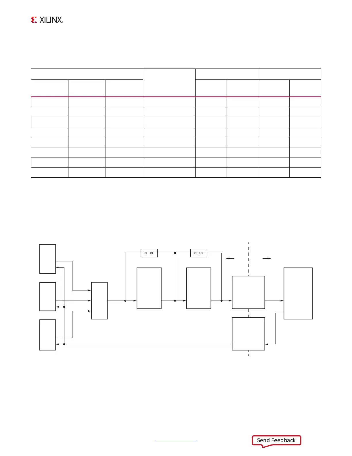
The ZC702 board JTAG chain is shown in Figure 1-9.
Table 1-9: SDIO Connections to the XC7Z020 SoC
XC7Z020 (U1) Pin
Schematic
Net Name
Level Shifter (U61) SDIO Connector (J64)
Pin Name Bank
Pin
Number
(A) Pin
Number
(B) Pin
Number
Pin
Number
Pin
Name
PS_MIO15 500 E6 SDIO_SDWP N/A N/A 11 PROTECT
PS_MIO0 500 G6 SDIO_SDDET N/A N/A 10 DETECT
PS_MIO41 501 C8 SDIO_CMD_LS 4 20 2 CMD
PS_MIO40 501 E14 SDIO_CLK_LS 9 19 5 CLK
PS_MIO42 501 D8 SDIO_DAT2_LS 1 23 9 DAT2
PS_MIO45 501 B9 SDIO_DAT1_LS 7 16 8 DAT1
PS_MIO44 501 E13 SDIO_DAT0_LS 6 18 7 DAT0
PS_MIO43 501 B11 SDIO_CD_DAT3_LS 3 22 1 CD_DAT3
X-Ref Target - Figure 1-9
Figure 1-9: JTAG Chain Block Diagram
UG850_c1_09_062918
2.5V3.3V
FMC LPC
Connector
TDI
TDO
J3
U1
Zynq-7000
XC7Z020
SoC
TDI
TDO
SN74AVC1T45
Voltage
Translator
TDI TDO
U39
FMC LPC
Connector
TDI
TDO
J4
SPST Bus Switch
U25
N.C. N.C.
SPST Bus Switch
U26
SN74AVC1T45
Voltage
Translator
TDO TDI
U38
JTAG
Module
TDO
TDI
U23
JTAG
Header
TDO
TDI
J2
JTAG
Header
TDO
TDI
J58
3:1
Analog
Switch
U75
U76
U77