ZC702 Board User Guide www.xilinx.com 49
UG850 (v1.7) March 27, 2019
Feature Descriptions
User PS Switches
[Figure 1-2, near callout 18]
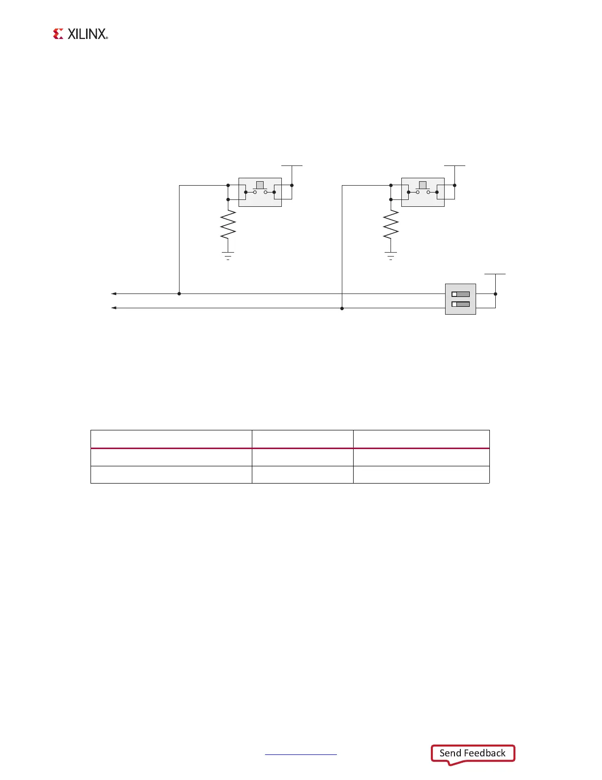
Figure 1-25 shows the user PS pushbutton and DIP switch circuit.
Table 1-26 lists the user PS-side pushbutton and DIP switch connections to XC7Z020 SoC
U1 Bank 500.
User PMOD GPIO Headers
[Figure 1-2, callout 28]
The ZC702 board supports two GPIO headers J62 and J63. The PMOD nets connected to
these headers are dual-purpose, with the User LEDs wired in parallel to the header pins.
J63 has a second dual-purpose function. The even numbered pins are wired in parallel to
the Arm PJTAG header J41 pins TDI, TIMS, TCK, and TDO. The J41 PJTAG signals are
connected to SoC Bank 13 GPIO pins which simultaneously drive J41 and J63. When J41 is
used for Arm PJTAG functionality, the J63 even numbered pin should not be used. When J63
even numbered pins are used as GPIO, connector J41 should not be used.
X-Ref Target - Figure 1-24
Figure 1-24: User PS Pushbutton and DIP Switch Circuit
Table 1-26: User PS Switch Connections to XC7Z020 SoC U1
XC7Z020 SoC (U1) Pin Net Name Switch and Pin Reference
B6 PS_DIP_SW0 SW13.4 and SW15.1
C5 PS_DIP_SW1 SW14.4 and SW15.2
VCCMIO_PS (1.8V)
R413
4.7 kΩ
0.1
Ω
5%
GND
4
32
1
SW13
UG850_c1_24_032719
VCCMIO_PS (1.8V)
R414
4.7 kΩ
0.1
Ω
5%2719
GND
4
32
1
SW14
PS_DIP_SW0
PS_DIP_SW1
1
2
4
VCCMIO_PS (1.8V)
3
SW15
SDA02H1SBD