ZC702 Board User Guide www.xilinx.com 68
UG850 (v1.7) March 27, 2019
Jumpers
Jumpers
[Figure 1-2, callout 24]
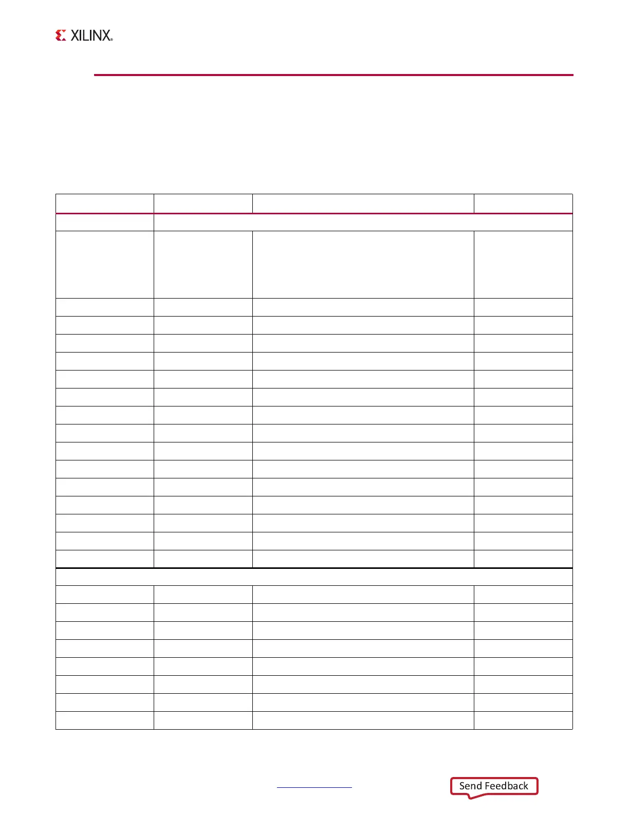
Default jumper positions are listed in Table A-2. Jumper locations are shown in Figure A-1.
Table A-2: Default Jumper Settings
Callout Jumper Function Default Position
HDR_1 X 2
1J5CFGBVS short to GND
ZC702 configuration bank 0 is operated at
2.5V, therefore the CFGBVS pin is pulled high
with a resistor. Jumper J5 should be never
installed.
OFF
2J6POR Master Reset
OFF
3 J7 USB 2.0 USB_VBUS_SEL
1-2
4J8XADC GND L3 BYPASS
OFF
5J9XADC GND
ON
6 J10 ARM HDR J41 PIN 2 TO VADJ
OFF
7 J11 UCD9248 U32 ADDR52 RESET_B
OFF
8J12 FMC VADJ OFF
ON
9 J13 UCD9248 U33 ADDR53 RESET_B
OFF
10 J14 UCD9248 U34 ADDR54 RESET_B
OFF
11 J15 CAN BUS COMMON-MODE CANH HDR
1-2
12 J43 ETHERNET PHY HDR
1-2
13 J44 USB 2.0 USB_RESET_B
OFF
14 J53 CAN BUS COMMON-MODE CANL HDR
1-2
15 J56 JTAG HDR J58 PIN 2 3.3V SEL
OFF
16 J65 XADC_VCC5V0 = VCC5V0
ON
HDR_1 X 3
17 J20 MIO3/QSPI_IO1
OFF
18 J21 MIO2/QSPI_IO0
OFF
19 J22 MIO4/QSPI_IO2
OFF
20 J25 MIO5/QSPI_IO3
OFF
21 J26 MIO6/QSPI_CLK
OFF
22 J27 PS_SRST_B
1-2
23 J28 PS_POR_B
1-2
24 J30 ETHERNET PHY HDR
1-2