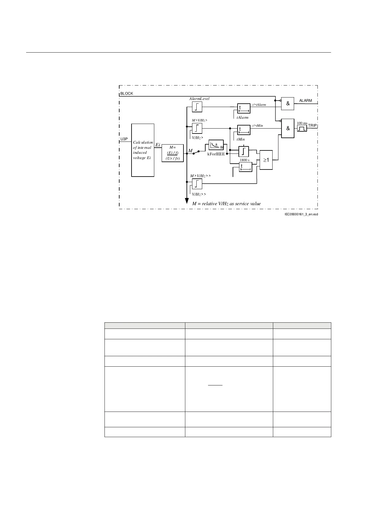
9.4.7.6 Logic diagram
IEC09000161_3_en.vsd
t
t
t
1
&
&
Ei
M=
(Ei / f)
(Ur / fr)
M = relative V/Hz as service value
V/Hz>>
M>V/Hz>>
V/Hz>
M>V/Hz>
tAlarm
tMin
kForIEEE
Calculation
of internal
induced
voltage Ei
k
M
M
t>tAlarm
t>tMin
ALARM
AlarmLevel
1800 s
U3P
BLOCK
100 ms
TRIP
IEC09000161 V3 EN
Figure 141: A simplified logic diagram of the Overexcitation protection
OEXPVPH
Simplification of the diagram is in the way the IEEE delays are calculated. The
cooling process is not shown. It is not shown that voltage and frequency are separately
checked against their respective limit values.
9.4.8 Technical data
Table 177: OEXPVPH technical data
Function
Range or value Accuracy
Operate value, start (100–180)% of (
UBase
/f
rated
) ± 0.5% of U
Operate value, alarm (50–120)% of start level ± 0.5% of U
r
at U ≤ U
r
± 0.5% of U at U > U
r
Operate value, high level (100–200)% of (
UBase
/f
rated
) ± 0.5% of U
Curve type IEEE
EQUATION1319 V1 EN (Equation 93)
where M = (E/f)/(Ur/fr)
± 5% + 40 ms
Minimum time delay for inverse
function
(0.000–60.000) s ± 0.5% ± 25 ms
Alarm time delay (0.00–9000.00) ± 0.5% ± 25 ms
Section 9 1MRK 502 048-UEN A
Voltage protection
284
Technical manual