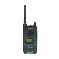
HM135 Service Manual
Preliminary version Page 4 of 13
2 CIRCUIT DESCRIPTION
2.1 General information
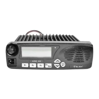
The HM135 is basically divided into 2 printed circuit boards: Main board and Head. Circuitry and signals can be
divided in the following sections:
Microprocessor/control
Front panel (head) circuitry
VCO / Synthesizer (PLL)
Transmitter
Receiver
Errore. L'origine riferimento non è stata trovata.
ON/OFF switch, rear connector and internal connectors
Refer to the Block Diagram and the Schematics.
2.2 Microprocessor/control
The microprocessor DD5 is constantly operating when the radio is turned ON. It is continuously monitoring the
keyboard, the PTT line and other internal inputs such as the squelch detect, etc. When a change occurs, the
microprocessor makes the appropriate response according to its program in order to control the all radio
functions. On channel change, the Radio emits a beep and the synthesizer is loaded with the correct frequency
information. The microprocessor runs off a 8 MHz oscillator which is composed of X3, C353, C354 and R319.
When the radio is first turned on, the microprocessor reads the radio status from the EEPROM DD3 which
contains all the radio’s parameters.
The microprocessor determinates the receive frequency codes, then loads the synthesizer via its pins 42 (line
PLL_LE), 43 (line PLL_DATA) and 46 (line PPL_CLK).
Pin 40 outputs a PWM signal which is converted by DA18:B into a CC voltage at its output (line RF_PWR_CTRL)
which controls the RF output power.
Pins 37 and pin 39 outputs a PWM signal which are used, respectively, to generate the Selcall signal (line
MCU_SELCALL_PWM) and CTCSS/DCS signal (line MCU_CTCSS_DCS_PWM) as further explained. The
digital signals coming from the ADC converters which drive the microprocessor in order to decode the Selcall and
CXTCSS/DCS signals are applied, respectively, to pin 59 (line ADC_HI_SPEED_DATA_RX) and pin 60
(ADC_lo_SPEED_DATA_RX).
The firmware program interface is made by means of the connector XP3
The microprocessor is fitted with an internal program flash memory as well, therefore functions can be
customized, if necessary, upon specific request from the customer.
2.2.a PTT circuit
The PTT switching is totally controlled by the two microprocessors (DD5 in the main board and DD800 in the front
board in the front panel): when the PTT is pressed, the line AUX_PTT goes low, so the transistor VT806 changes
the status of the pin 20 of microprocessor DD800 which is “informed” that the radio is in TX mode (i.e. PTT is
pressed), so it changes its output at pin 22 putting the low level at pin 8 of the connector XT802 which is
connected to the main PCB with the connector XT2. This means that pin 8 of XT2 (line
HANDSET_PTT_TO_MPU) goes low. This line is connected to the VT56 which changes the status of pin 26 of
the microprocessor DD5 from hi to low. Now the microprocessor DD5 is also “informed” that the radio is in TX
mode, so it can control the +8V voltage which is alternatively fed to the TX or RX stages according to the radio’s
status. Pins 29 (line TX_FROM_MCU) and 30 (line RX_FROM_MCU) control the +8V power switches which
alternatively outputs this voltage to the RX section (line +8V_RX) with VT42 or to the TX one (line +8V_TX) with
VT41.
The transistor VT805 is controlled by the pin 19 of the microprocessor DD800 and it is used to eventually disable
all the over stated PTT chain according to the radio’s status (e.g. busy lock out, timeout timer etc).