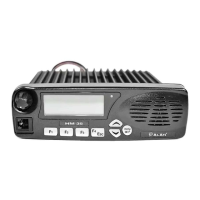
HM135 Service Manual
Preliminary version Page 7 of 13
2.5.d Transmitter Audio Circuits
The speech audio coming from the MIC connector (line AUX_MIC) is applied to the FET VT804 which acts as
sensitivity switch (function high/low MIC sensitivity) in 2 levels and is directly controlled by the microprocessor (pin
27) via the transistor VT807. The signal is then fed to the amplifier made by DA801:A (DA801:B is used to supply
the reference voltage at its positive input) providing a stronger speech signal (line MIC_INPUT) which is fed to the
6dB per octave pre-emphasis circuit provided by the capacitor C277 and the resistor R213 and applied to pin 6 of
DA11:B.
NOTE: Between the C277 and the MIC_INPUT line, the transistor VT48 acts as a mute switch which disable the speech
audio when a Selcall is sent.
Selcall audio PWM signaling coming from the pin 37 of the microprocessor (line MCU_SELCALL_PWM) is fed to
the 3 KHz low pass filter which consists of DA9:B and related circuitry. Its output is then fed to the input of the
DA11:B, so routed the same way of the speech audio.
The speech/Selcall signal is applied to the input of DA11:B which limits the peak-to-peak output, then is fed to the
pin 3 of IC DA10 which is a double digital audio regulator. After the level regulation, the speech/Selcall is output at
pin 11 and sent to the first input (pin 9) of DA9:C in order to be summed with the CTCSS/DCS signal.
NOTE: The level regulation of DA10 comes in form of digital data from the pins 6, 7 and 8 (lines POT_DATA, POT_CLK
and DAC_CS respectively) which are directly controlled by the microprocessor DD5 (pins 43, 46 and 36 respectively) via
related logical inverters.
CTCSS/DCS sub-audio tone PWM signaling coming from the pin 39 of the microprocessor (line
MCU_CTCSS_DCS_PWM) is fed to the CTCSS/DCS 300 Hz low pass filter which consists of DA9:A and related
circuitry, then fed in the pin 2 of the IC DA10 which regulates the level and outputs the regulated CTCSS/DCS at
its pin 12. This signal is then applied to the second input of DA9:C in order to be summed with the speech/Selcall
signal.
DA9:C sums the two signals (speech/Selcall coming from pin 11 of DA10 and CTCSS/DCS coming from pin 12)
feeding its combined output to DA9:D which is a 3 KHz low pass filter. The output of DA9:D is then applied to pins
4 and 5 of the DA10.
2.5.e Double-point modulation
The outputs (lines REF_MOD and VCO_MOD) coming, respectively, from pins 10 and 9 of DA10 are fed to the
PLL area. The line REF_MOD is directly applied to the trimmer RP3 which provides the Ref. Modulation control
(low audio frequencies) directly applied to the TCXO. The line VCO_MOD is applied via the resistors R116 to the
trimmer RP4 which provides the VCO modulation control (high audio frequencies) directly sent to the TX VCO.
2.6 Receiver
2.6.a Receiver’s Front-End
The RX signal coming from the antenna connector is fed in sequence through the coupling line TA1, the low pass
filter (consisting of L46 to L49 and connected capacitors) and the antenna switching (VD21 and VD22). The
output of the antenna switching (line RF_RX) is sent to input of the receiver and coupled to the input band-pass
filter. The transistor VT2 is the front-end amplifier and its output is applied to the second band-pass filter (L2, L3,
L4, L5 and related capacitors). The output from the band-pass filter is applied to the pin 4 of the RF mixer A1.
The diode VD1 is used for the function local/distance. Normally the line LOCAL_DIST issued by the pin 25 of the
microprocessor (properly adapted by R317 and C352) goes to high so VT1 is switched on forward biasing the
diode VD1. This provides a bypass of the resistor R5 for the RF, so the RF signal fed to the mixer is higher
(distance mode). On the other side, if the line LOCAL_DIST drops to low, the diode VD1 is not forward biased and
the RF is attenuated of 10dB approx. due to the R5 (local mode).
2.6.b Local Oscillator (LO)
As already explained in the PLL section, the output coming from the RX VCO (working at 45,1 MHz above the RX
frequency) is sent to the synthesizer buffer VT19, then sent to DA5 for an additional buffering. The output of DA5
is connected to the low-pass filter (L27, L28, L29 and related capacitors), then sent to the RX stages (line
HET_RX) which is sent to the RX mixer A1 via an attenuator which consists of R13, R14 and R15.