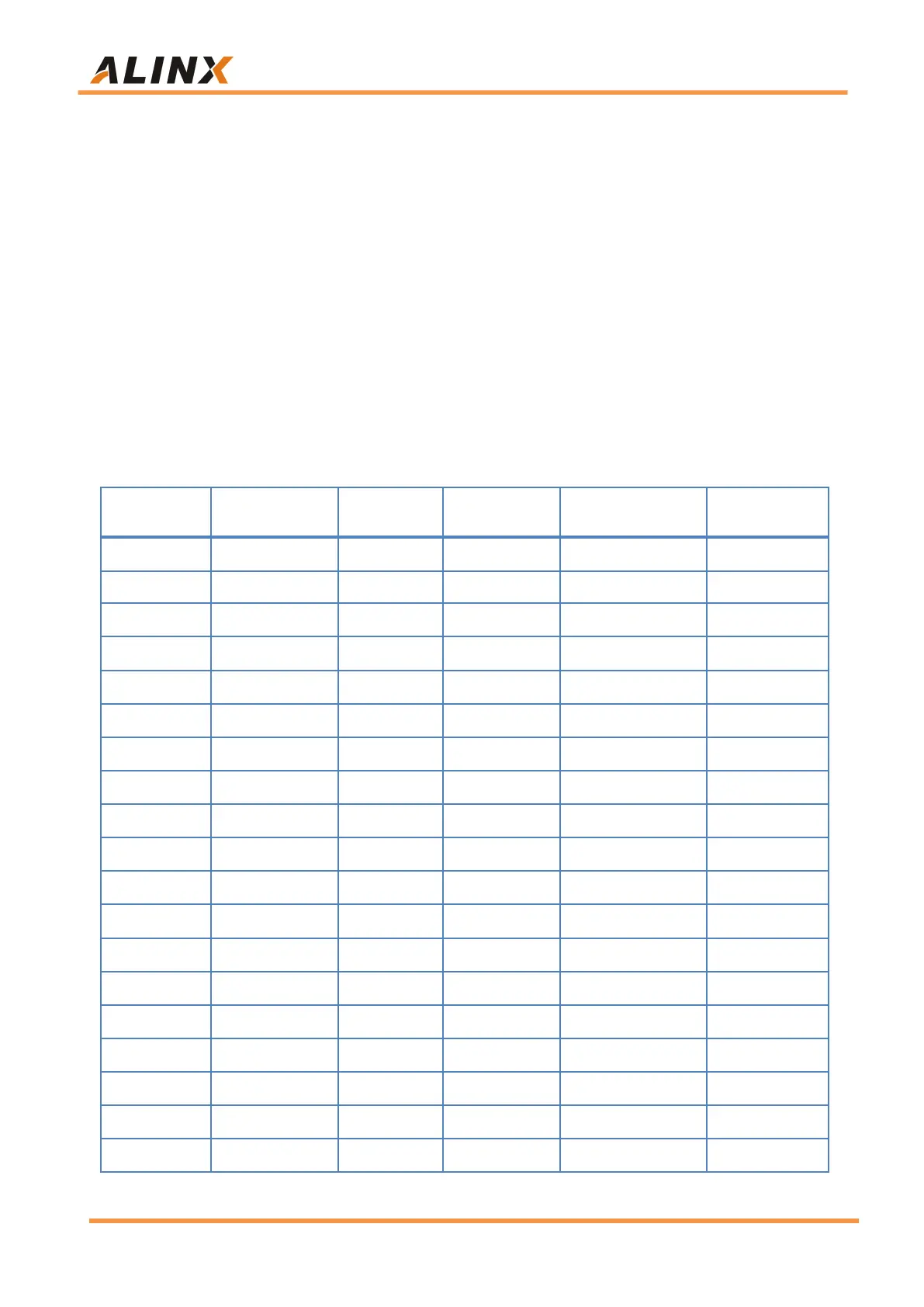
them, J29 is connected to the IO of BANK65 and BANK66, J30 is connected to
the IO of BANK25, BANK26, BANK66 and the transceiver signal of BANK505
MGT, J31 is connected to the IO of BANK24 and BANK44, J32 is connected to
the MIO, VCCO_65, VCCO_66 and +12V power supply of PS.
Among them, the IO level standard of BANK43~46 is 3.3V, and the
level standard of BANK65 and BANK66 is determined by the VCCO_65
and VCCO_66 power supply of the carrier board, but cannot exceed +1.8V;
the level standard of MIO is also 1.8V.
Pin assignment of board to board connector J29