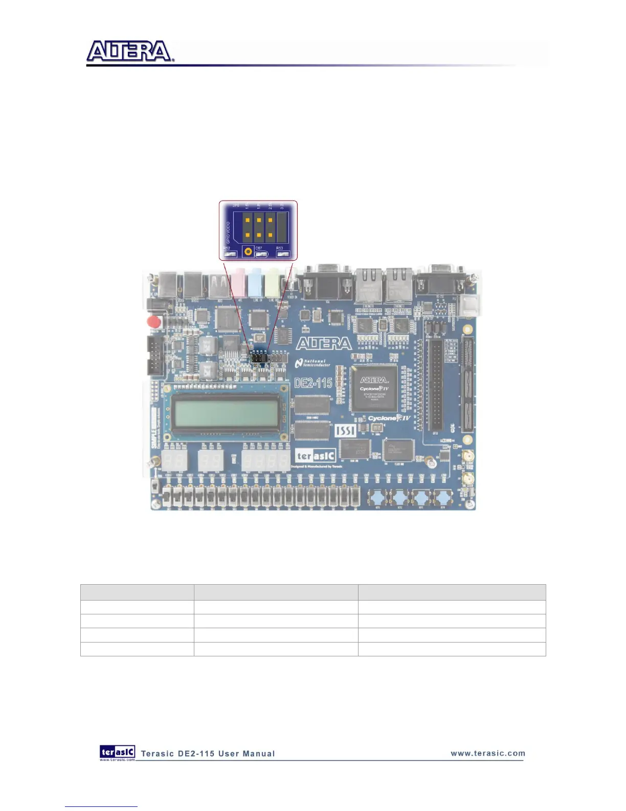
The voltage level of the I/O pins on the expansion headers can be adjusted to 3.3V, 2.5V, 1.8V, or
1.5V using JP6 (The default value is 3.3V, see Figure 4-17). Because the expansion I/Os are
connected to Bank 4 of the FPGA and the VCCIO voltage (VCCIO4) of this bank is controlled by
the header JP6, users can use a jumper to select the input voltage of VCCIO4 to 3.3V, 2.5V, 1.8V,
and 1.5V to control the voltage level of the I/O pins. Table 4-11 lists the jumper settings of the JP6.
The pin-outs of the JP6 appear in Figure 4-17.
Figure 4-17 GPIO VCCIO supply voltage setting header
Table 4-11 Voltage Level Setting of the Expansion Headers Using JP6