Note : Users who want to use daughter card on GPIO connector need to pay close attention
to the I/O standard between DE2-115 GPIO connector pins and daughter card system. For
example, if the I/O standard of GPIO pins on DE2-115 board is set to 1.8V, a daughter card with
3.3V I/O standard may not work properly on the DE2-115 board due to I/O standard mismatch.
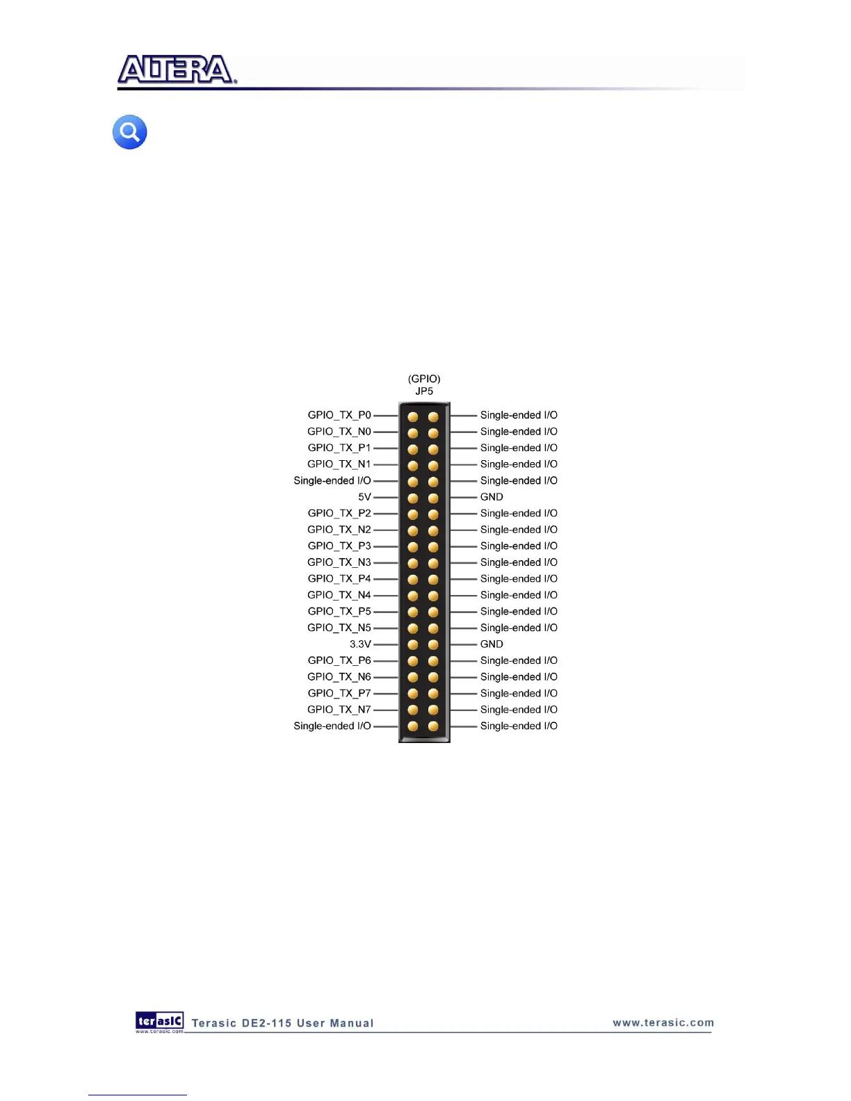
Figure 4-18 depicts the pin definition on the expansion connector for using these I/Os as LVDS
transmitters. Due to the reason that the column I/Os of the FPGA the expansion pins connecting
with can only support emulated LVDS transmitters, two single-ended output buffers and external
resistors must be used as shown in Figure 4-19. The associated I/O standard of these differential
FPGA I/O pins on Quartus II project should set to LVDS_E_3R.
Figure 4-18 Pin defined when using LVDS interface on GPIO FPGA pins
The factory default setting on Rs resistor will be 47 ohm and Rp resistor will not be assembled for
single-ended I/O standard application. For LVDS transmitter application, please assemble 120 and
170 ohm resistor on Rs and Rp position, respectively.
Finally, Table 4-12 shows all the pin assignments of the GPIO connector.