EasyManua.ls Logo

Arrow CYC5000 - Peripherals Connected to the FPGA; Communication and Configuration; Figure 4 - CYC5000 Clock Tree

Arrow CYC5000
70 pages
Print Icon
To Next Page IconTo Next Page
To Previous Page IconTo Previous Page
Loading...
CYC5000 User Guide www.arrow.com
Page | 11 March 2023
Board
Reference
FPGA Pin No.
Pin Func.
Description
I/O Std
CLK12M
PIN_F14
Input
12MHz clock input
3.3 V
REFCLK
PIN_G14
Input
Optional clock input
3.3 V
3.3 Peripherals Connected to the FPGA
3.3.1 Communication and Configuration
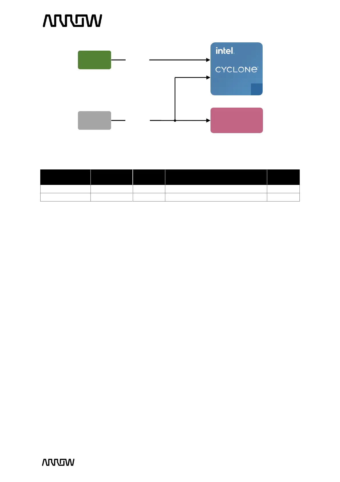
The CYC5000 board uses a single chip to perform configuration of the device and communication
over USB.
3.3.1.1 USB Communication
The FTDI chip converts signals from USB 2.0 to a variety of standard serial and parallel interfaces.
Channel A of FTDI chip is used in MPPSE mode for JTAG. Channel B is routed to FPGA and is
usable for other standard interfaces.













Figure 4 CYC5000 Clock Tree

Table of Contents