CYC5000 User Guide www.arrow.com
Page | 8 March 2023
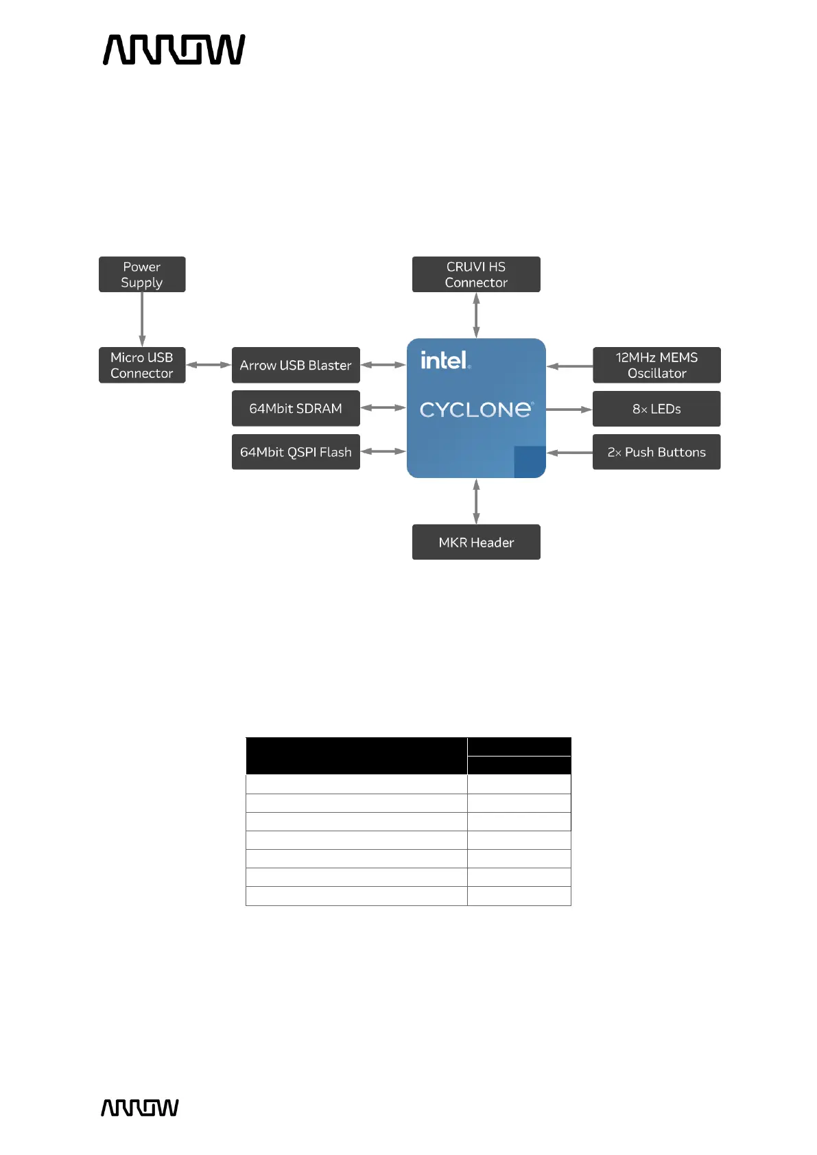
2.2 Block Diagram
Figure 2 represents the block diagram of the board. All the connections are established through
the Cyclone V FPGA device to provide maximum flexibility for users. Users can configure the
FPGA to implement any system design.
FPGA Device
• Intel Cyclone V 5CEBA2U15C8N device.
Features of the FPGA on the CYC5000 Board: