4.3.1. Atmel AVR UC3 On-chip Debug System
The Atmel AVR UC3 OCD system is designed in accordance with the Nexus 2.0 standard (IEEE-ISTO
5001
™
-2003), which is a highly flexible and powerful open on-chip debug standard for 32-bit
microcontrollers. It supports the following features:
• Nexus compliant debug solution
• OCD supports any CPU speed
• Six program counter hardware breakpoints
• Two data breakpoints
• Breakpoints can be configured as watchpoints
• Hardware breakpoints can be combined to give break on ranges
• Unlimited number of user program breakpoints (using BREAK)
• Real-time program counter branch tracing, data trace, process trace (supported only by debuggers
with parallel trace capture port)
For more information regarding the AVR UC3 OCD system, consult the AVR32UC Technical Reference
Manuals, located on www.atmel.com/uc3.
4.3.2. JTAG Physical Interface
The JTAG interface consists of a 4-wire Test Access Port (TAP) controller that is compliant with the IEEE
®
1149.1 standard. The IEEE standard was developed to provide an industry-standard way to efficiently test
circuit board connectivity (Boundary Scan). Atmel AVR and SAM devices have extended this functionality
to include full Programming and On-chip Debugging support.
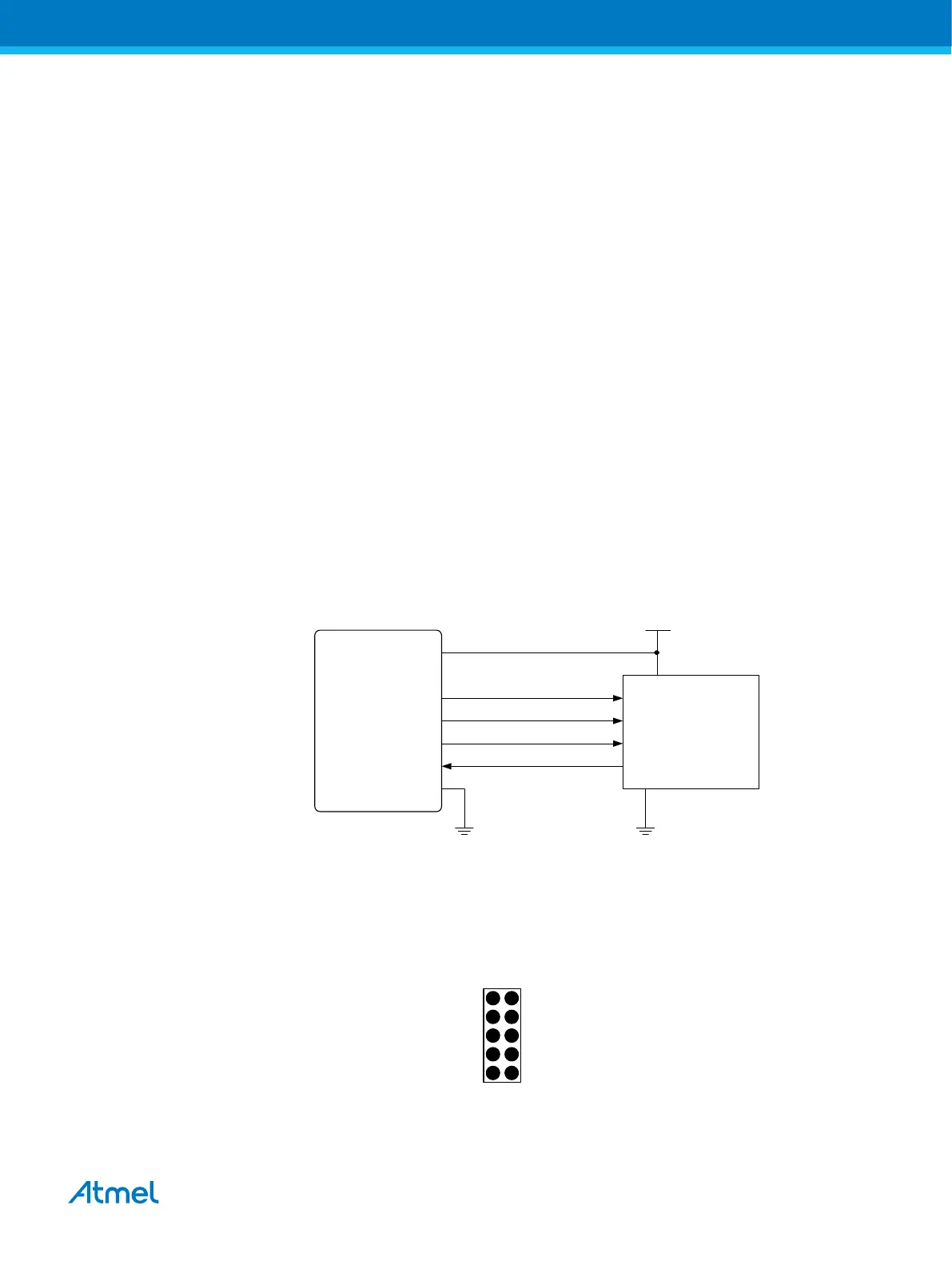
Figure 4-5. JTAG Interface Basics
Vcc
TMS
TDI
TDO
TCK
programmer /
debugger
Atmel
target
device
4.3.2.1. AVR JTAG Pinout
When designing an application PCB, which includes an Atmel AVR with the JTAG interface, it is
recommended to use the pinout as shown in the figure below. Both 100-mil and 50-mil variants of this
pinout are supported, depending on the cabling and adapters included with the particular kit.
Figure 4-6. AVR JTAG Header Pinout
GND
VCC
/RESET
(TRST)
GND
TCK
TDO
TMS
TDI
1 2
AVR JTAG
(NC)
Atmel Atmel-ICE [USER GUIDE]
Atmel-42330C-Atmel-ICE_User Guide-10/2016
30

 Loading...