81
8126F–AVR–05/12
ATtiny13A
• Bits 1:0 – ACIS[1:0]: Analog Comparator Interrupt Mode Select
These bits determine which comparator events that trigger the Analog Comparator interrupt. The
different settings are shown in Table 13-2 on page 81.
When changing the ACIS1/ACIS0 bits, the Analog Comparator Interrupt must be disabled by
clearing its Interrupt Enable bit in the ACSR Register. Otherwise an interrupt can occur when the
bits are changed.
13.2.3 DIDR0 – Digital Input Disable Register 0
• Bits 1:0 – AIN1D, AIN0D: AIN[1:0] Digital Input Disable
When this bit is written logic one, the digital input buffer on the AIN1/0 pin is disabled. The corre-
sponding PIN Register bit will always read as zero when this bit is set. When an analog signal is
applied to the AIN1/0 pin and the digital input from this pin is not needed, this bit should be writ-
ten logic one to reduce power consumption in the digital input buffer.
Table 13-2. ACIS1/ACIS0 Settings
ACIS1 ACIS0 Interrupt Mode
0 0 Comparator Interrupt on Output Toggle.
01Reserved
1 0 Comparator Interrupt on Falling Output Edge.
1 1 Comparator Interrupt on Rising Output Edge.
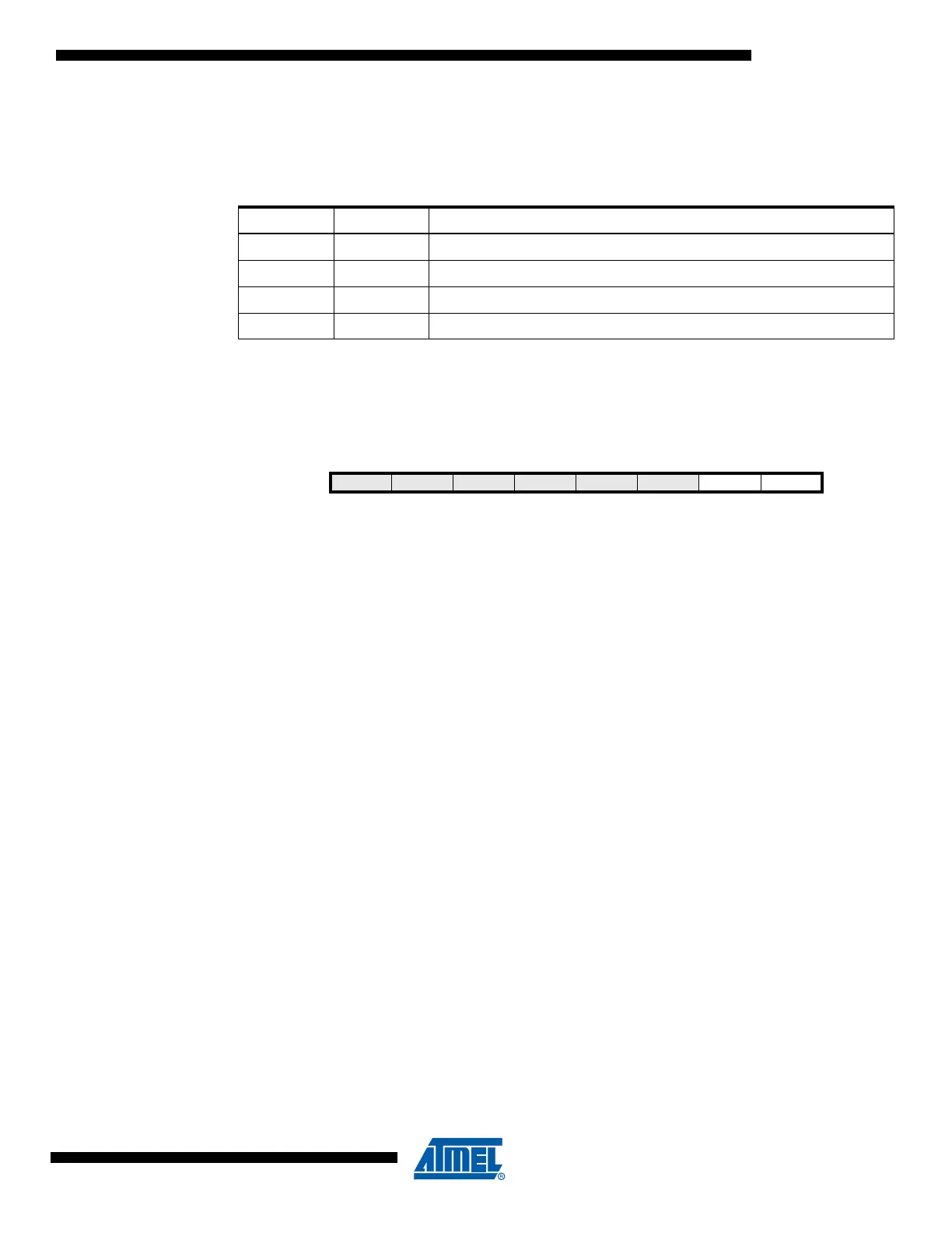
Bit 76543210
0x14
– – ADC0D ADC2D ADC3D ADC1D AIN1D AIN0D DIDR0
Read/Write R R R/W R/W R/W R/W R/W R/W
Initial Value00000000