16
ATtiny26(L)
1477G–AVR–03/05
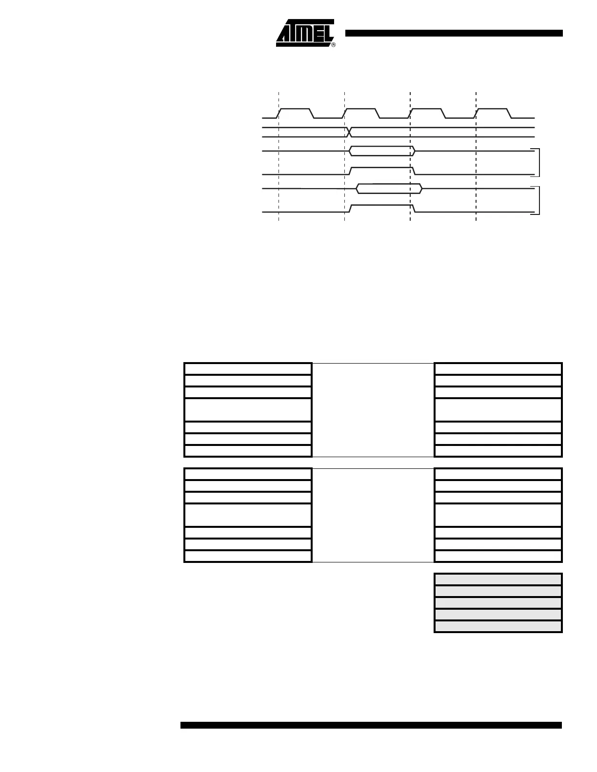
Figure 18. On-chip Data SRAM Access Cycles
In-System Programmable
Flash Program Memory
The ATtiny26(L) contains 2K bytes On-chip In-System Programmable Flash memory for
program storage. Since all instructions are 16- or 32-bit words, the Flash is organized as
1K x 16. The Flash memory has an endurance of at least 10,000 write/erase cycles. The
ATtiny26(L) Program Counter – PC – is 10 bits wide, thus addressing the 1024 program
memory addresses, see “Memory Programming” on page 107 for a detailed description
on Flash data downloading. See “Program and Data Addressing Modes” on page 10 for
the different program memory addressing modes.
Figure 19. SRAM Organization
SRAM Data Memory Figure 19 above shows how the ATtiny26(L) SRAM Memory is organized.
The lower 224 Data Memory locations address the Register File, the I/O Memory and
the internal data SRAM. The first 96 locations address the Register File and I/O Mem-
ory, and the next 128 locations address the internal data SRAM.
ystem Clock Ø
WR
RD
Data
Data
Address
Address
Prev. Address
Register File Data Address Space
R0 $0000
R1 $0001
R2 $0002
... ...
R29 $001D
R30 $001E
R31 $001F
I/O Registers
$00 $0020
$01 $0021
$02 $0022
… …
$3D $005D
$3E $005E
$3F $005F
Internal SRAM
$0060
$0061
...
$00DE
$00DF