128
ATtiny26(L)
1477G–AVR–03/05
External Clock Drive
Waveforms
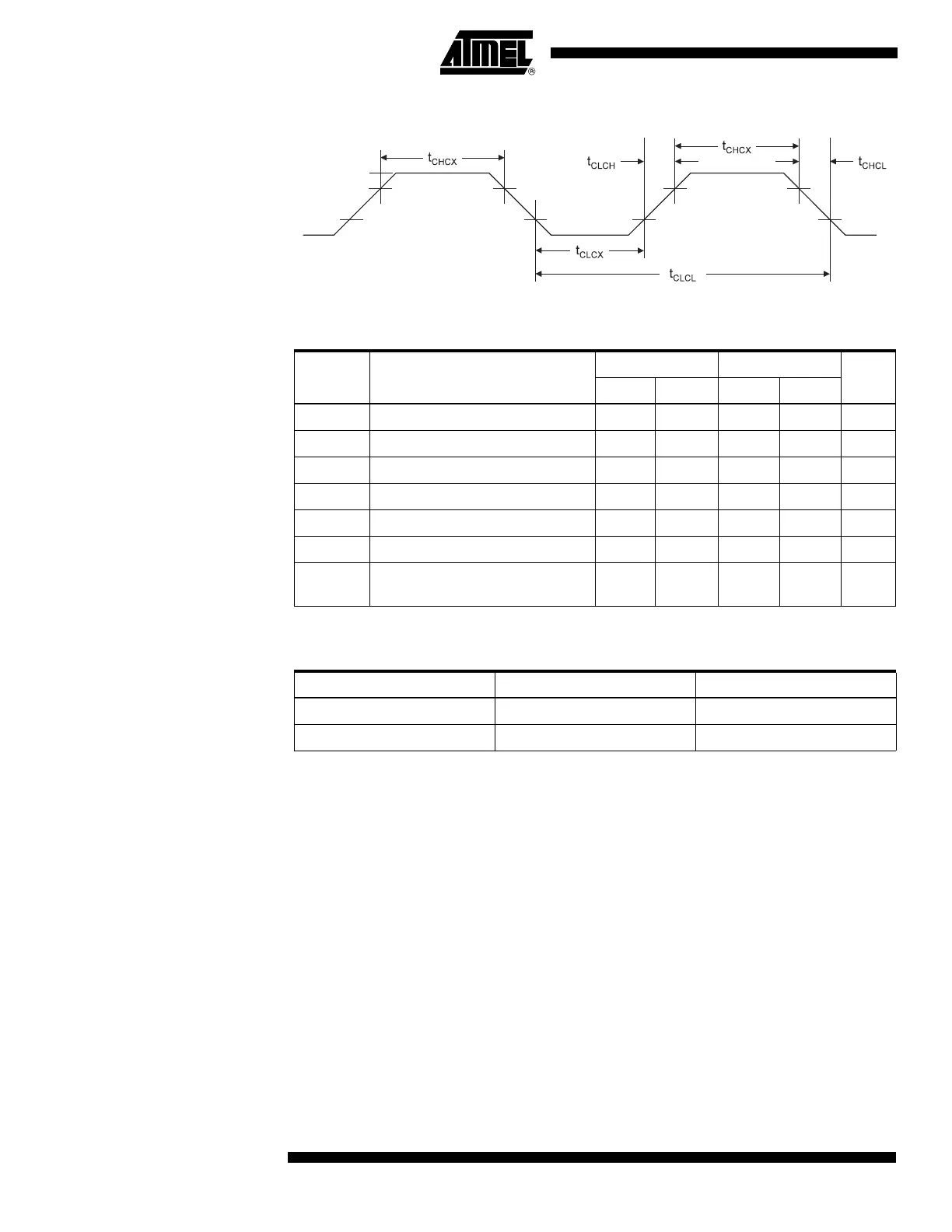
Figure 70. External Clock Drive Waveforms
External Clock Drive
Notes: 1. R should be in the range 3 kΩ - 100 kΩ, and C should be at least 20 pF. The C values
given in the table includes pin capacitance. This will vary with package type.
2. The frequency will vary with package type and board layout.
V
IL1
V
IH1
Table 63. External Clock Drive
Symbol Parameter
V
CC
= 2.7 - 5.5V V
CC
= 4.5 - 5.5V
UnitsMin Max Min Max
1/t
CLCL
Oscillator Frequency 0 8 0 16 MHz
t
CLCL
Clock Period 125 62.5 ns
t
CHCX
High Time 50 25 ns
t
CLCX
Low Time 50 25 ns
t
CLCH
Rise Time 1.6 0.5 µs
t
CHCL
Fall Time 1.6 0.5 µs
∆t
CLCL
Change in period from one clock
cycle to the next
22
Table 64. External RC Oscillator, Typical Frequencies
R [kΩ]
(1)
C [pF] f
(2)
33 22 650 kHz
10 22 2.0 MHz